


Quick Research
Generate reliable direction feasibility study reports for your R&D in just a few steps.

Technical Q&A
Discover and master advanced knowledge NOW. Basics, ideas, possibilities, all at once.

Find Solutions
As an expert in R&D theories, this can generate solutions to your technical problems instantly.

Evaluate Feasibility
Analyze your overall solution with one click, know your potential R&D risks in advance.

Monitor Landscape
Get weekly tech updates, stay abreast of the latest tech innovations and key insights.
Registration method and system for circuit design layout and electron microscope scanning image, circuit design layout and imaging error calculation method thereof
A technique for electron microscope scanning and circuit design, which is applied in computing, image enhancement, image analysis, etc., can solve problems such as circuit design layout and electron microscope scanning image registration difficulties, and achieve accurate error calculation, fast and accurate registration, and accurate registration Effect
- Summary
- Abstract
- Description
- Claims
- Application Information
AI Technical Summary
Problems solved by technology
Method used
Image


Examples
no. 1 example
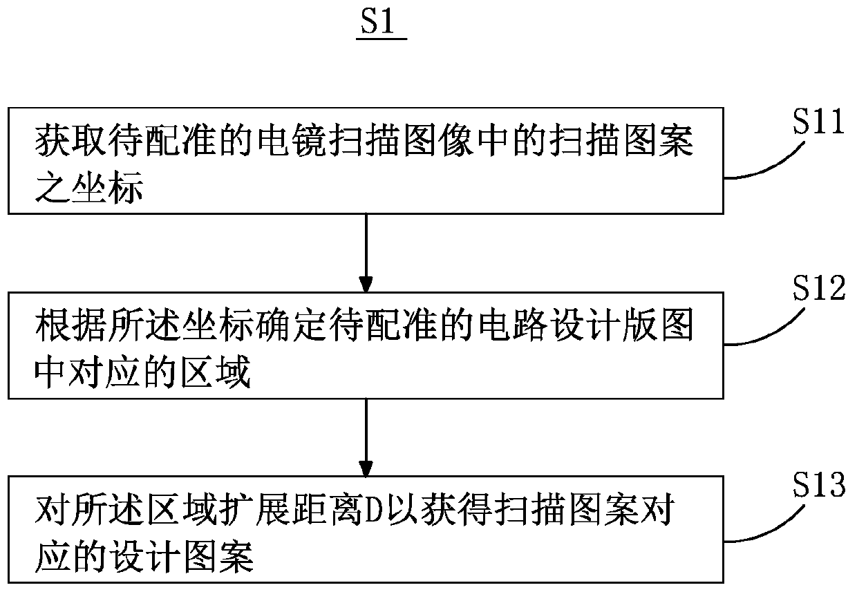
[0035] see figure 1 , The first embodiment of the present invention provides a method 10 for registering a circuit design layout and a scanning electron microscope image, through which the circuit design layout and its corresponding scanning electron microscope image can be registered.
[0036] The registration method 10 of the circuit design layout and the scanning electron microscope image includes:
[0037] Step S1: providing a circuit design layout to be registered and an electron microscope scan image, the circuit design layout to be registered includes at least one design pattern, and the electron microscope scan image to be registered includes at least one scan pattern corresponding to the at least one design pattern ; The design pattern covers its corresponding scanning pattern;
[0038] Step S2: Process the circuit design layout to be registered to obtain the design version Figure II value image, the design version Figure II The grayscale value in the design patte...
Embodiment approach
[0061] see Figure 4B , as another implementation, step Sb1 includes:
[0062] Step Sb1-1': corroding the electron microscope scanning image to be registered; and
[0063] Step Sb1-2': Obtain the outline of the scan pattern through an edge detection algorithm in image processing.
[0064] Since the scan pattern outline in the electron microscope scan image usually has a certain width, which will lead to inaccurate acquisition of the scan image outline, in step Sb1-1', the electron microscope scan image to be registered is etched to refine the scan pattern outline width , to avoid the situation of two edges in edge detection.
[0065] see Figure 4C , as a specific implementation, in step Sb1, adaptive threshold binarization is used to extract the contour, which includes:
[0066] Step Sb1-a: setting the grayscale threshold; and
[0067] Step Sb1-b: comparing the pixel values of the pixels of the electron microscope scanning image to be registered with the gray threshold...
no. 2 example
[0075] see Figure 6 , the second embodiment of the present invention provides a registration system 20 of a circuit design layout and an electron microscope scanning image. The registration system 20 of a circuit design layout and an electron microscope scanning image includes an input module 21, a binary image processing module 22, and a Gaussian filter module 23 and registration module 24.
[0076]The input module 21 is used to input and provide the circuit design layout to be registered and the scanning electron microscope image, the circuit design layout to be registered includes at least one design pattern, and the scanning electron microscope image to be registered includes at least one pattern corresponding to the at least one design pattern. A scan pattern; the design pattern covers its corresponding scan pattern.
[0077] The binary image processing module 22 is used to process the circuit design layout to be registered to obtain the design version Figure II value ...
PUM
 Abstract
Description
Claims
Application Information
 - R&D Engineer
- R&D Manager
- IP Professional
- Industry Leading Data Capabilities
- Powerful AI technology
- Patent DNA Extraction
Browse by: Latest US Patents, China's latest patents, Technical Efficacy Thesaurus, Application Domain, Technology Topic, Popular Technical Reports.
© 2024 PatSnap. All rights reserved.Legal|Privacy policy|Modern Slavery Act Transparency Statement|Sitemap|About US| Contact US: help@patsnap.com