Multichannel gate-all-around transistor

A multi-channel, transistor technology, used in transistors, semiconductor devices, electrical components, etc., can solve the problems of easy breakdown driving power, large parasitic capacitance, etc., and achieve good radiation resistance, small off-state current density, good resistance to radiation. The effect of total dose-response capacity

Inactive Publication Date: 2020-07-21
SHANGHAI INST OF MICROSYSTEM & INFORMATION TECH CHINESE ACAD OF SCI
View PDF5 Cites 2 Cited by
  • Summary
  • Abstract
  • Description
  • Claims
  • Application Information

AI Technical Summary

Problems solved by technology

[0015] In view of the above-mentioned shortcomings of the prior art, the purpose of the present invention is to provide a multi-channel gate-around transistor, which is used to solve the problems of large parasitic capacitance, easy breakdown and low driving power of the gate-around transistor in the prior art

Method used


Image

  • Multichannel gate-all-around transistor
  • Multichannel gate-all-around transistor
  • Multichannel gate-all-around transistor

Examples


Embodiment 1

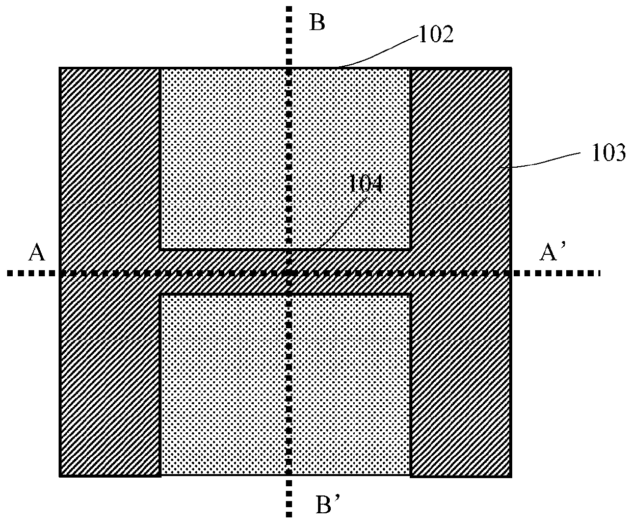
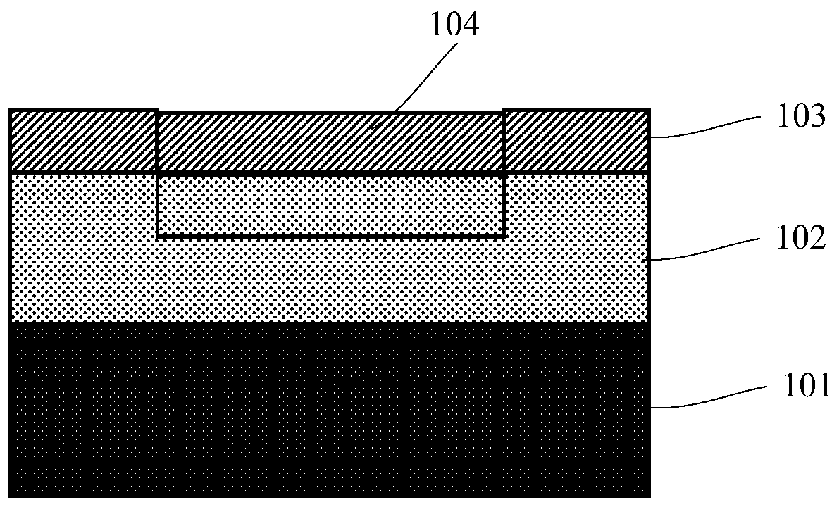
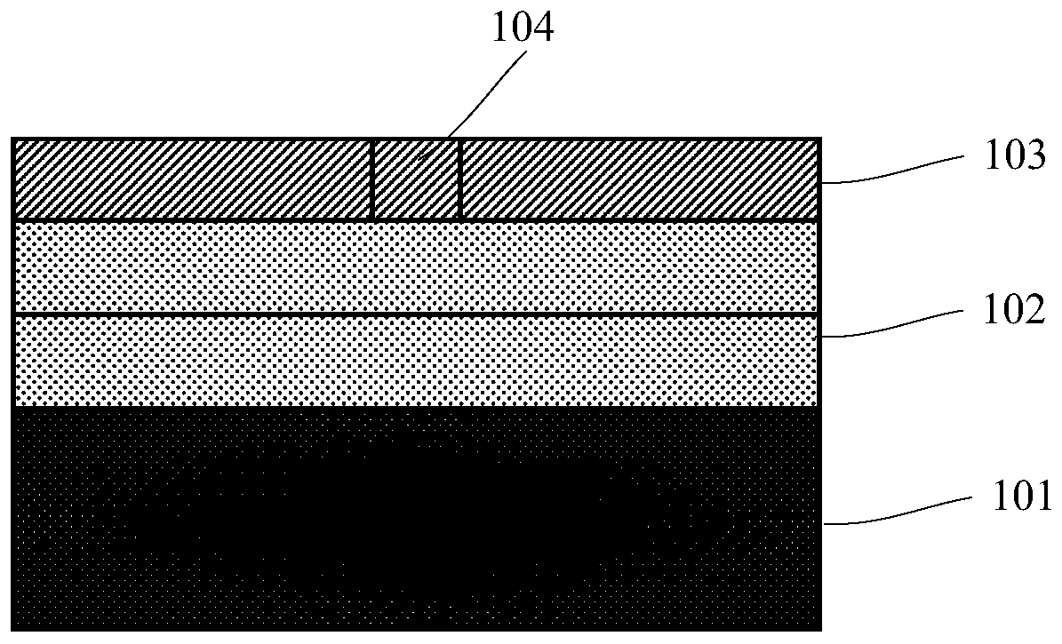
[0051] Such as Figure 15 ~ Figure 17 As shown, among them, Figure 16 shown as Figure 15 The schematic diagram of the cross-sectional structure at A-A' in the middle, Figure 17 shown as Figure 15 Schematic diagram of the cross-sectional structure at B-B' in the middle. This embodiment provides a multi-channel gate-all-round transistor, including: a semiconductor substrate 201, an insulating layer 202, a semiconductor nanowire structure, a gate dielectric layer 601, a gate electrode layer 602, a source region 603 and a drain region 604, a source electrode 605 and Drain electrode 606 .

[0052] The semiconductor substrate 201 may be a silicon substrate, a silicon carbide substrate, a gallium nitride substrate, or the like.

[0053] There is a groove in the insulating layer 202 , and the groove does not penetrate through the insulating layer 202 . As an example, the thickness of the insulating layer 202 is not greater than 150 nanometers, and the depth of the groove is ...

Embodiment 2

[0068] Such as Figure 19 ~ Figure 22 As shown, this embodiment provides a three-dimensional stacked multi-channel gate-around transistor, wherein, Figure 19 shown as Figure 18 The schematic diagram of the cross-sectional structure at A-A' in the middle, Figure 20 shown as Figure 18 Schematic diagram of the cross-sectional structure at B-B' in the middle. The basic structure of the multi-channel gate-all-around transistor of this embodiment is the same as that of Embodiment 1, wherein the difference from Embodiment 1 is that the gate-all-round transistor comprises a plurality of semiconductor nanowire structures stacked upwards, and the nanowire structure It includes semiconductor protrusions located on both sides of the groove and a plurality of semiconductor nanowires connected to the semiconductor protrusions, and two adjacent semiconductor protrusions are separated by sacrificial layer protrusions 608, so that the upper and lower There is an interval between two ad...


PUM

PropertyMeasurementUnit
thicknessaaaaaaaaaa
depthaaaaaaaaaa

Abstract

The invention provides a multichannel gate-all-around transistor. The multichannel gate-all-around transistor comprises: a semiconductor substrate; an insulating layer which is provided with a groovewhich does not penetrate through the insulating layer; a semiconductor nanowire structure which is suspended in the air, stretches across the groove and comprises semiconductor bosses located on the two sides of the groove and a plurality of semiconductor nanowires connected to the bosses; a gate dielectric layer and a gate electrode layer which surround the semiconductor nanowires; a source region and a drain region which are formed at the end parts of the semiconductor nanowires, wherein the plurality of semiconductor nanowires between the semiconductor bosses form a multichannel channel region together; and a source electrode and a drain electrode. The width of the groove below the multichannel gate-all-around transistor is smaller than that of the semiconductor nanowires, so that an unnecessary overlapping region between the bottom gate and the source drain can be effectively avoided, the scattering of carriers in a channel is reduced, the parasitic capacitance of the source drainis reduced, and the high-frequency characteristic of the device is improved. The gate-all-around transistor is provided with a plurality of channels, the driving power of the transistor can be greatlyimproved, and the integration level of a device is improved.

Description

technical field [0001] The invention belongs to the field of design and manufacture of semiconductor integrated circuits, in particular to a multi-channel gate-around transistor and a preparation method thereof. Background technique [0002] As microelectronic devices continue to shrink, it is expected that the existing FinFET technology will face a large technical bottleneck at the 5nm and 3nm nodes, and the device performance will no longer be greatly improved as the device size continues to decrease. This requires us to adopt new device technologies, such as new device materials (such as strained silicon, silicon germanium, germanium, III-V semiconductors, etc.), and new device structures (such as nanowire gate-around transistors, etc.). [0003] The nanowire gate-all-around transistor can confine the conductive channel to the center of the nanowire, rather than the interface between the nanowire and the gate oxide layer, which greatly reduces the scattering of carriers. ...

Claims


Application Information

Patent Timeline
Patent Type & Authority Applications(China)
IPC IPC(8): H01L29/775H01L29/786H01L29/423B82Y10/00
CPCB82Y10/00H01L29/42392H01L29/775H01L29/78696
Inventor 刘强俞文杰任青华陈治西刘晨鹤赵兰天陈玲丽王曦
Owner SHANGHAI INST OF MICROSYSTEM & INFORMATION TECH CHINESE ACAD OF SCI
Why Eureka
Try Eureka