
Three-dimensional NAND flash memory device and preparation method thereof

A flash memory, three-dimensional technology, applied in electrical components, electrical solid devices, circuits, etc., can solve problems such as difficulty in forming embedded chips, and achieve the effect of improving space utilization efficiency and reducing horizontal occupied area

Inactive Publication Date: 2020-07-17
SIEN QINGDAO INTEGRATED CIRCUITS CO LTD
View PDF0 Cites 0 Cited by
  • Summary
  • Abstract
  • Description
  • Claims
  • Application Information

AI Technical Summary

Problems solved by technology

[0004] In view of the above-mentioned shortcoming of prior art, the object of the present invention is to provide a kind of three-dimensional NAND flash memory device and preparation method thereof, be used to solve the 3D NAND flash memory device of the multi-layer NAND storage string with vertical alignment channel in the prior art Difficulty in forming embedded chips etc.

Method used


Image

  • Three-dimensional NAND flash memory device and preparation method thereof
  • Three-dimensional NAND flash memory device and preparation method thereof
  • Three-dimensional NAND flash memory device and preparation method thereof

Examples


Embodiment 1

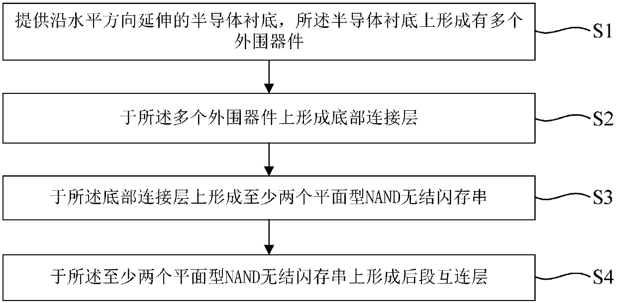
[0082] Such as figure 1 As shown, the present embodiment provides a method for preparing a three-dimensional NAND flash memory device. In this embodiment, a planar NAND junction-free flash memory string (i.e., a two-dimensional charge trap junctionless field-effect transistor flash memory) structure is combined with a peripheral device (i.e., a PUC, Peri Under Cell) are combined to build a three-dimensional NAND flash memory device. The fast read characteristics of the planar NAND junction-free flash memory string are well utilized, and it is well compatible with the logic unit, so it can be well applied in the embedded NAND flash memory device, and can also be made as a standard independent NAND flash memory products; on the other hand, PUC technology is used to stack the peripheral circuits used to drive the planar NAND junction-free flash memory strings under the planar NAND junction-free flash memory strings for storing data. The required parking lot is rebuilt from the s...

Embodiment 2

[0101] Such as Figure 14 to Figure 15 as shown, Figure 15 for Figure 14 The structure shown is a top view of the structure layer of the planar NAND junction-free flash memory string 22. The purpose is to clearly express the horizontal distribution of the planar NAND junction-free flash memory string 22. This embodiment provides a three-dimensional NAND flash memory device. The three-dimensional NAND flash memory device can be prepared by the preparation method described in Example 1, or by other methods, which are not limited here. The three-dimensional NAND flash memory device includes at least:

[0102] a semiconductor substrate 20 extending in the horizontal direction, on which a plurality of peripheral devices are formed;

[0103] a bottom connection layer 21, the bottom connection layer 21 is formed on the peripheral device;

[0104] At least two planar NAND junction-free flash memory strings 22, the at least two planar NAND junction-free flash memory strings 22 ar...


PUM


Abstract

The invention provides a three-dimensional NAND flash memory device and a preparation method thereof. The preparation method comprises the steps of providing a semiconductor substrate extending alongthe horizontal direction, and forming a plurality of peripheral devices on the semiconductor substrate; forming a bottom connection layer on the plurality of peripheral devices; forming at least two planar NAND junctionless flash memory strings on the bottom connecting layer; and forming a back-end interconnection layer on the at least two planar NAND junctionless flash memory strings; combining aplanar NAND junctionless flash memory string structure with a peripheral device to construct the three-dimensional NAND flash memory device. According to the present invention, the quick reading characteristic of the planar NAND junctionless flash memory strings is well utilized, the planar NAND junctionless flash memory strings can be well compatible with a logic unit, a standard independent NAND flash memory product can be manufactured, but also an embedded NAND flash memory product can be manufactured according to the use condition under the condition that the product performance is guaranteed; and on the other hand, by adopting the mode, the horizontal occupied area of the two-dimensional NAND flash memory device can be effectively reduced, and the space use efficiency of the device is improved.

Description

technical field [0001] The invention relates to the field of semiconductor storage devices, in particular to a three-dimensional NAND flash memory device and a preparation method thereof. Background technique [0002] With the continued emphasis on highly integrated electronics, there is a continuing need for semiconductor memory devices that operate at higher speeds and lower power and have increased device densities. In order to improve the density of memory, the industry has made extensive efforts to develop methods for reducing the size of two-dimensionally arranged memory cells. As the size of memory cells of two-dimensional (2D) memory devices continues to decrease, its manufacturing process encounters various challenges: physical limits, such as exposure technology limits, development technology limits, and storage electron density limits, etc., resulting in conflicts and interferences in storage signals significantly increased, making it difficult to perform multi-l...

Claims


Application Information

Patent Timeline
IPC IPC(8): H01L27/115H01L27/11573H01L27/1157H01L27/11582
CPCH10B69/00H10B43/40H10B43/35H10B43/27
Inventor 肖德元张汝京
Owner SIEN QINGDAO INTEGRATED CIRCUITS CO LTD
Learn More