Wafer bump and manufacturing method of wafer bump

A manufacturing method and wafer technology, applied in semiconductor/solid-state device manufacturing, electrical components, electrical solid-state devices, etc., can solve problems such as metals are easily oxidized

Inactive Publication Date: 2020-07-07
CHIPMORE TECH CORP LTD
View PDF5 Cites 0 Cited by
  • Summary
  • Abstract
  • Description
  • Claims
  • Application Information

AI Technical Summary

Problems solved by technology

[0004] The purpose of the present invention is to provide a wafer bump and a method for manufacturing the wafer bump, so as to solve the problem that the metal on the existing wafer bump is easily oxidized

Method used


Image

  • Wafer bump and manufacturing method of wafer bump
  • Wafer bump and manufacturing method of wafer bump
  • Wafer bump and manufacturing method of wafer bump

Examples


Embodiment Construction

[0028] In order to make the object, technical solution and advantages of the present invention clearer, the present invention will be described in detail below in conjunction with the accompanying drawings and specific embodiments.

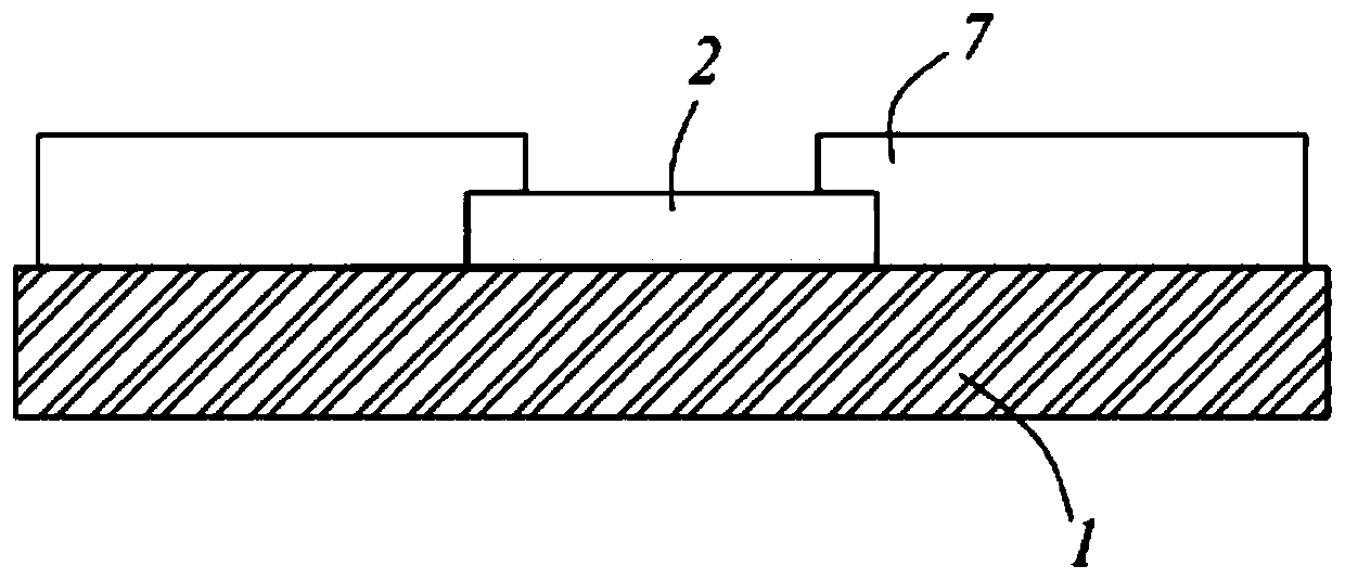
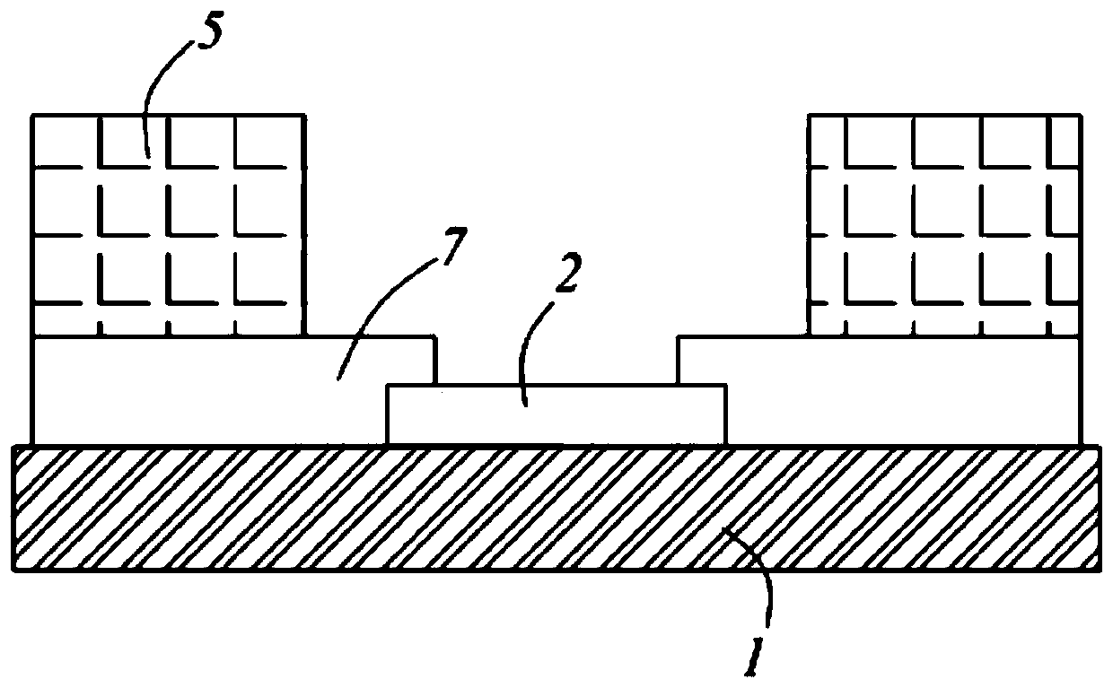
[0029] Such as Figure 6 As shown, the wafer bump 100 of the present invention includes a semiconductor substrate 1 located at the bottom, a protective layer 7 located on the semiconductor substrate 1, a circuit layer embedded in the protective layer 7 and exposed from the protective layer 7 2. The first metal layer 3 and the second metal layer 4 located on the circuit layer 2 , the first photoresist 5 and the isolation layer 6 arranged around the side of the first metal layer 3 .

[0030] The material of the semiconductor substrate 1 may be silicon or gallium arsenide and the like.

[0031] The height of the protective layer 7 is higher than that of the circuit layer 2, and the middle part of the protective layer 7 forms an exposed space, and th...


PUM


Abstract

The invention provides a wafer bump and a manufacturing method of the wafer bump. The wafer bump comprises a semiconductor substrate located at the bottom, a circuit layer located on the semiconductorsubstrate, a first metal layer and a second metal layer; wherein the first metal layer and the second metal layer are located above the circuit layer; the first metal layer is located between the second metal layer and the circuit layer, the wafer bump further comprises a first photoresist arranged around the side surface of the first metal layer and an isolation layer located between the first metal layer and the circuit layer, and the height of the first photoresist is not lower than that of the first metal layer. The wafer bump can prevent the first metal layer from being oxidized. The manufacturing method of the wafer bump is simple in process, the manufactured wafer bump is high in oxidation resistance, and the galvanic effect caused by the potential difference between the two kindsof metal can be resisted.

Description

technical field [0001] The invention relates to a wafer bump and a method for manufacturing the wafer bump to solve the problem that the metal layer on the existing wafer bump is easily oxidized and the problem of the Giavani effect due to the existence of different metals. Background technique [0002] The exposed metal on the existing wafer bumps is prone to oxidation, which in turn affects product characteristics. In addition, because there are different metal layers on the wafer bump, the different metals generate current through the medium due to the potential difference, and then an electrochemical reaction occurs, causing part of the metal to be oxidized, that is, the Giavani effect. , which will affect the reliability of the product. [0003] In view of this, it is necessary to improve the existing wafer bumps and wafer bump manufacturing methods to solve the above problems. Contents of the invention [0004] The object of the present invention is to provide a wa...

Claims


Application Information

Patent Timeline
Patent Type & Authority Applications(China)
IPC IPC(8): H01L23/488H01L21/60
CPCH01L24/11H01L24/13H01L2224/1302H01L2224/13022H01L2224/13144H01L2224/13147H01L2224/13155H01L23/488
Inventor 陈浩
Owner CHIPMORE TECH CORP LTD
Why Eureka
Try Eureka