Light-emitting element array structure and manufacturing method of light-emitting element array structure

A technology of light-emitting element and array structure, which is applied in the direction of electrical components, electric solid-state devices, semiconductor devices, etc., can solve the problems of insufficient flatness of the surface of the solder resist layer, affecting the thickness uniformity of the light-emitting element and pad strength and electrical performance, etc. , to achieve the effect of improving the bonding yield

Pending Publication Date: 2020-06-19
同扬光电(江苏)有限公司
View PDF0 Cites 0 Cited by
  • Summary
  • Abstract
  • Description
  • Claims
  • Application Information

AI Technical Summary

Problems solved by technology

The surface flatness of the solder resist layer formed by the above method is insufficient
In addition, the poor flatness of the solder resist layer will affect its thickness uniformity and the strength and electrical performance of the joint between the light-emitting element and the pad

Method used


Image

  • Light-emitting element array structure and manufacturing method of light-emitting element array structure
  • Light-emitting element array structure and manufacturing method of light-emitting element array structure
  • Light-emitting element array structure and manufacturing method of light-emitting element array structure

Examples


Embodiment Construction

[0042] Reference will now be made in detail to the exemplary embodiments of the present invention, examples of which are illustrated in the accompanying drawings. Wherever possible, the same reference numbers will be used in the drawings and description to refer to the same or like parts.

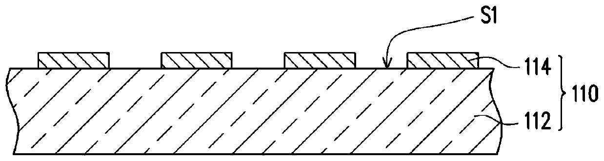
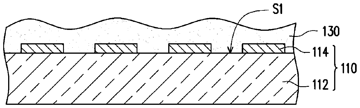
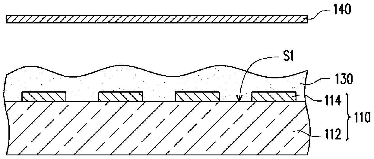
[0043] Figure 1 to Figure 6 It is a schematic cross-sectional view of part of the process of a method for fabricating a light-emitting element array structure according to an embodiment of the present invention.

[0044] Please refer to figure 1 , in this embodiment, the manufacturing method of the light-emitting element array structure includes the following steps. First, a substrate 110 is provided. The substrate 110 may include a dielectric layer 112 and a patterned circuit layer 114 , wherein the dielectric layer 112 has an upper surface S1 , and the patterned circuit layer 114 is located on the upper surface S1 of the dielectric layer 112 . The substrate 110 can be a rigid substra...


PUM

PropertyMeasurementUnit
surface roughnessaaaaaaaaaa
hardnessaaaaaaaaaa

Abstract

The invention provides a manufacturing method of a light-emitting element array structure. The manufacturing method comprises the following steps: providing a substrate, wherein the upper surface of the substrate is provided with a patterned circuit layer; forming an insulating film layer on the substrate, wherein the insulating film layer covers the upper surface and the patterned circuit layer;providing a release film on the insulating film layer; performing a hot pressing process to press the release film so as to flatten the surfaces of the release film and the insulating film layer, thepressing pressure of the hot pressing process being between 5 kg / cm<2> and 15 kg / cm<2>; performing a patterning process on the planarized insulating film layer to form a patterned insulating film layer, the patterned insulating film layer including a plurality of openings arranged in an array to expose a portion of the patterned circuit layer; and arranging a plurality of light-emitting elements on the patterned insulating film layer in an array mode, and enabling the light-emitting elements to be electrically connected with the patterned circuit layer through the openings, wherein the size ofthe light-emitting elements is smaller than or equal to 200 micrometers. The invention also provides a light-emitting element array structure.

Description

technical field [0001] The invention relates to a light-emitting element array structure and a manufacturing method of the light-emitting element array structure. Background technique [0002] Traditional light-emitting diodes are mostly used as backlights for liquid crystal display devices or directly as light-emitting pixels. However, due to insufficient resolution, the latter are mostly used in large-scale advertising light panels, and are rarely used in consumer electronics products. [0003] In recent years, a new display technology has been developed—submillimeter light-emitting diode (Mini LED) and micro-light-emitting diode (Micro LED), which mainly miniaturize, thin-film, and array LED, and its size is on the order of microns. When the above-mentioned light-emitting element array configured in an array is applied to display technology, how to tightly bond a large number of light-emitting elements in an array to the substrate becomes very important. However, in the ...

Claims


Application Information

Patent Timeline
Patent Type & Authority Applications(China)
IPC IPC(8): H01L27/15
CPCH01L27/156
Inventor 刘逸群洪培豪贾孟寰沈建成李远智
Owner 同扬光电(江苏)有限公司
Why Eureka
Try Eureka