Memory device and fault repairing method thereof

A fault repair and memory technology, applied in the field of integrated circuits, can solve the problems that the repair requirements cannot be fully covered, and the time-consuming of memory fault repair cannot be ignored.

Pending Publication Date: 2020-06-19
UNIV OF ELECTRONICS SCI & TECH OF CHINA
View PDF7 Cites 12 Cited by
  • Summary
  • Abstract
  • Description
  • Claims
  • Application Information

AI Technical Summary

Problems solved by technology

[0005] In the traditional redundant repair schemes implemented by fuse programming technology and laser fusing technology, the programming of decoders and redundant resources is a one-time and irreversible programming. Therefore, for the above-mentioned storage array block scheme and many similar memory architecture designs, when the faulty storage units in two sub-storage blocks have conflicting requirements for redundant resources, the traditional redundancy repair scheme cannot fully cover the repairs in each sub-storage array block need
In addition, with the advancement of semiconductor manufacturing technology, the feature size of semiconductor integrated circuits is getting smaller and smaller, which poses a huge challenge to the accuracy of laser fusing equipment for laser fuses; at the same time, with the increase in memory storage capacity, there may be The number of faulty cells has also increased, making the time-consuming use of laser fuse technology or electric fuse technology to repair memory faults cannot be ignored

Method used


Image

  • Memory device and fault repairing method thereof
  • Memory device and fault repairing method thereof
  • Memory device and fault repairing method thereof

Examples


Embodiment Construction

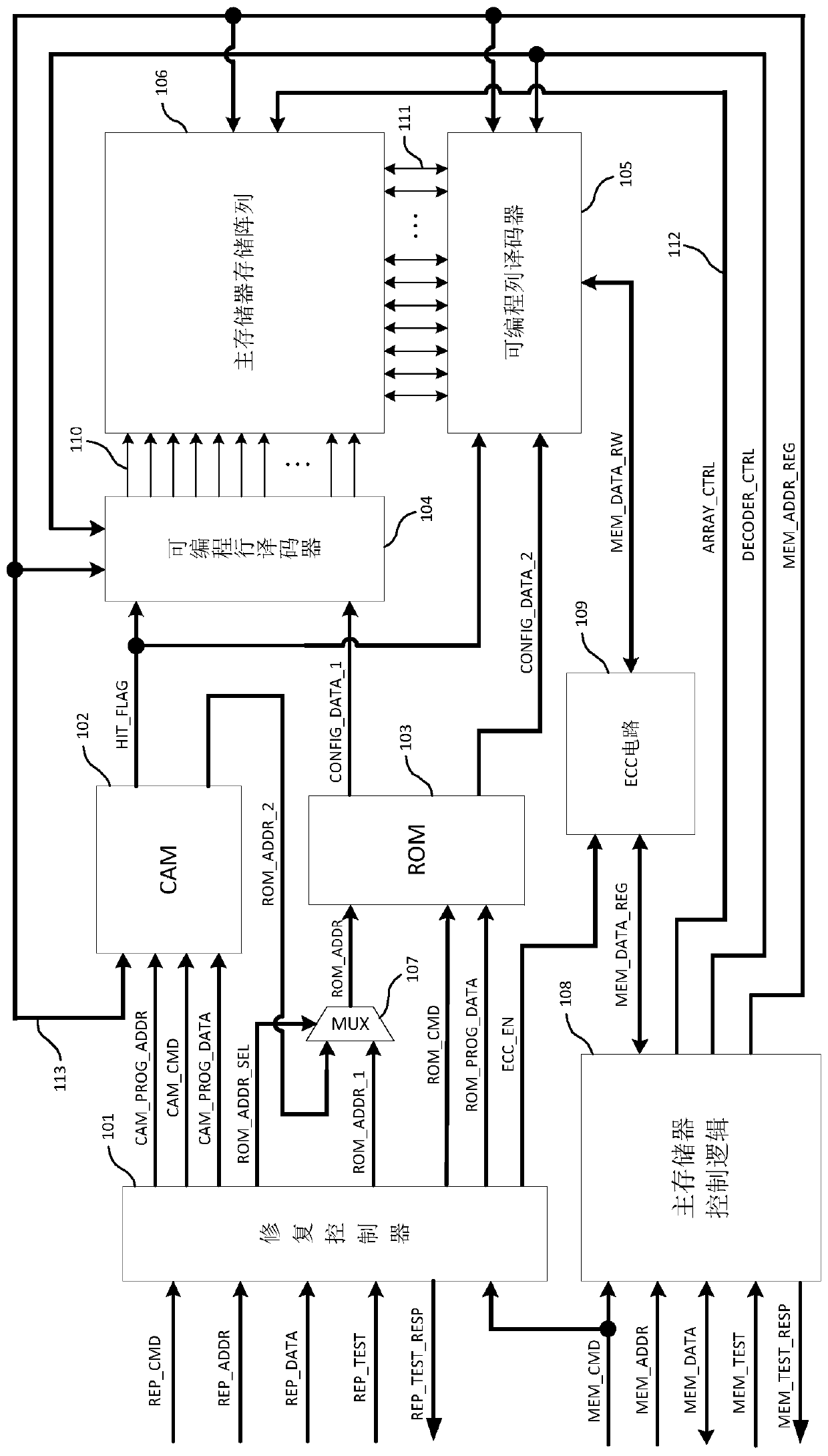
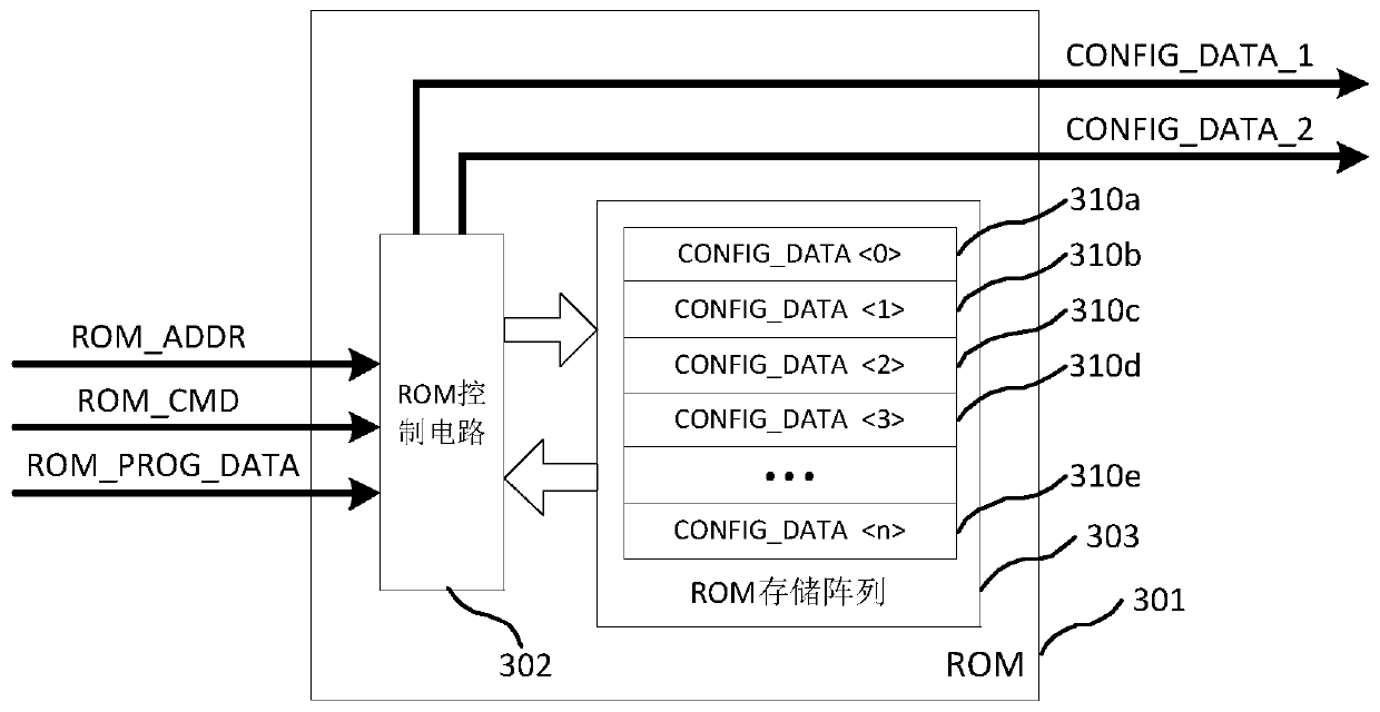
[0022] The following detailed description with respect to the accompanying drawings is intended as a description of present example embodiments of the invention and does not represent the only way in which the invention may be practiced. It should be understood that, although not described in detail, similar or equivalent functions can be performed by different embodiments within the spirit and scope of the present invention. In this article, the term "content addressable memory" is referred to by "CAM"; the term "read-only memory" is referred to by "ROM"; the term "main memory" refers to the memory that is repaired, and in practice, " "Main memory" includes many types, and its application objects can cover all semiconductors on the market or memories based on semiconductor integrated processes, such as SRAM, DRAM, FRAM, MRAM, PROM, etc.; the term "memory chip" refers to the tape-out but not diced , packaged memory chips; the term "next production link" refers to subsequent pr...


PUM


Abstract

A circuit architecture of a memory device includes: a main memory circuit for implementing storage of user data; and the main memory fault repair circuit is used for realizing repair of storage faultsin the main memory. The main memory circuit comprises a memory array circuit designed in an array partitioning mode. In a main memory failure repair circuit, a CAM is used to store a failure addressof a main memory, and an ROM is used to store configuration data for configuring a programmable address decoder in a main memory circuit. A memory fault repair method includes repair schemes for wordfaults, row faults, and column faults of a memory device. A memory fault test and fault repair process for fault detection, fault analysis, and fault repair prior to memory device packaging includes arepairability determination method of a memory device and an operating method of programming a fault repair circuit of the memory device.

Description

technical field [0001] The present invention relates to integrated circuits containing memories, and more particularly, to integrated circuits containing memories and requiring repair of defective memory cells in the memories. The present invention also relates to a storage failure recovery scheme, more specifically, a recovery scheme for storage failures caused by storage array failures and peripheral read-write circuit failures. Background technique [0002] During the manufacturing process of the semiconductor memory, due to process defects and other reasons, memory cells with physical defects appear in the memory array of the manufactured memory chip. The existence of defective memory cells will lead to the abnormal function of the produced memory chips under certain specific access addresses, and the inability to access data safely and effectively, thus making the memory chips invalid. Redundancy repair technology introduces redundant rows and redundant columns in the ...

Claims


Application Information

Patent Timeline
Patent Type & Authority Applications(China)
IPC IPC(8): G11C17/18G11C29/42G11C29/44
CPCG11C17/18G11C29/42G11C29/44
Inventor 王刚包王勇李威
Owner UNIV OF ELECTRONICS SCI & TECH OF CHINA
Why Eureka
Try Eureka