
Chip wafer test control method and device, and chip

A technology of wafer testing and control methods, applied in the field of microelectronics, can solve problems such as vulnerability to attacks and security impacts, and achieve high security and improved security effects

Pending Publication Date: 2020-06-09
DATANG MICROELECTRONICS TECH CO LTD
View PDF2 Cites 5 Cited by
  • Summary
  • Abstract
  • Description
  • Claims
  • Application Information

AI Technical Summary

Problems solved by technology

The traditional chip design has a certain design for the security part. Enter the password to enter the wafer test, but the password is fixed or stored in the chip, which is vulnerable to attack. After the wafer test is over, if the attacker breaks the password, he can still enter. wafer test mode, whereby security is compromised

Method used


Image

  • Chip wafer test control method and device, and chip
  • Chip wafer test control method and device, and chip
  • Chip wafer test control method and device, and chip

Examples


Embodiment Construction

[0037] The application describes a number of embodiments, but the description is illustrative rather than restrictive, and it will be obvious to those of ordinary skill in the art that within the scope of the embodiments described in the application, There are many more embodiments and implementations. Although many possible combinations of features are shown in the drawings and discussed in the detailed description, many other combinations of the disclosed features are possible. Except where expressly limited, any feature or element of any embodiment may be used in combination with, or substituted for, any other feature or element of any other embodiment.

[0038] This application includes and contemplates combinations of features and elements known to those of ordinary skill in the art. The disclosed embodiments, features and elements of this application can also be combined with any conventional features or elements to form unique inventive solutions as defined by the clai...


PUM


Abstract

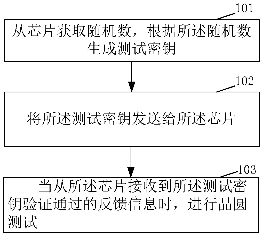
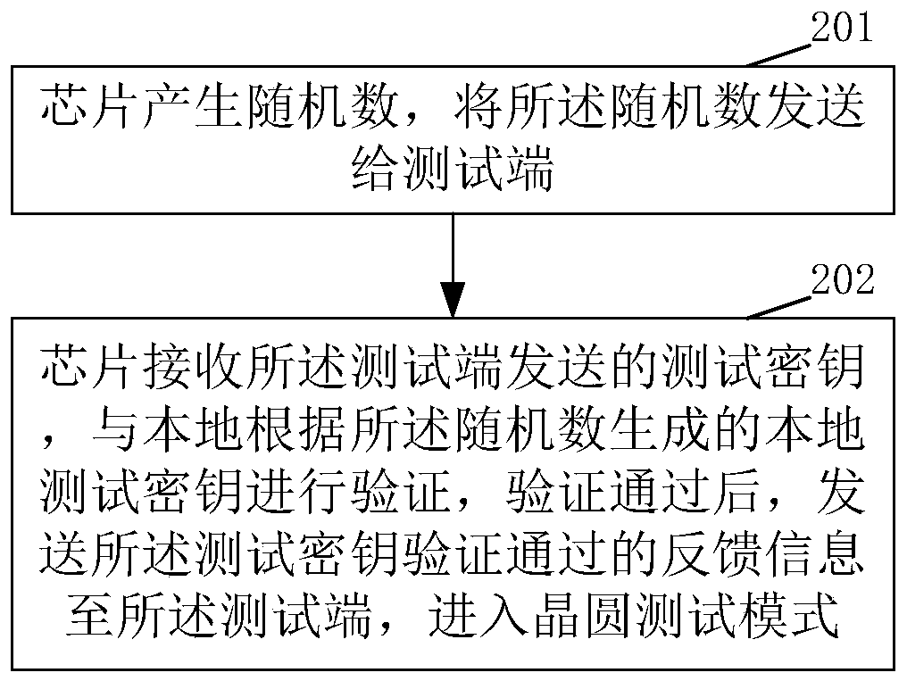
The invention discloses a chip wafer test control method and device and a chip. The chip wafer test control method comprises the steps of obtaining a random number from the chip, and generating a testsecret key according to the random number; and sending the test secret key to the chip; and when feedback information that the test secret key passes verification is received from the chip, carryingout wafer test. According to the scheme provided by the embodiment of the invention, the test password related to the random number generated by the chip is used, so that the security of the secret key generated in the mode is higher, and the attack difficulty is higher; besides, random numbers generated by different chips are generally different, so that test passwords are different; even if onechip is cracked, the chip cannot be directly applied to other chips; and the safety of the chip is improved.

Description

technical field [0001] This article relates to microelectronics technology, especially a chip wafer test control method and device, chip. Background technique [0002] Wafer testing is an important part of chip testing. The chip will update key data such as memory during the wafer test, which requires security control of the chip wafer test to prevent the chip from rewriting key data during use. [0003] Chip security design has always been the key to chip development and design. A good security design circuit is crucial to the security of the entire chip. It can increase the attack difficulty and attack time of the attacker, thereby improving the security of the chip. [0004] The traditional chip test circuit enters the wafer test by entering a set of passwords. After the wafer test is completed, a fixed key is written to the chip and stored in the memory. Due to the protection of the key, the memory instructions and data are encrypted , which has certain security and is...

Claims


Application Information

Patent Timeline
Patent Type & Authority Applications(China)
IPC IPC(8): H04L9/08G01R31/28G01R31/26
CPCH04L9/0869H04L9/0891G01R31/2851G01R31/2601
Inventor 韩晓晶
Owner DATANG MICROELECTRONICS TECH CO LTD
Learn More