
Additive for acid polishing of silicon wafer and application thereof

A silicon chip acid and additive technology, applied in the direction of crystal growth, single crystal growth, polycrystalline material growth, etc., can solve the problem that the back of the silicon chip is not flat enough, and achieve the effect of slowing down oxidation and dissolution

Active Publication Date: 2020-06-09
CHANGZHOU SHICHUANG ENERGY CO LTD
View PDF4 Cites 2 Cited by
  • Summary
  • Abstract
  • Description
  • Claims
  • Application Information

AI Technical Summary

Problems solved by technology

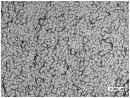
[0005] like figure 2 As shown, after conventional acid polishing on the back of the silicon wafer, the back of the silicon wafer is still not flat enough, and the conventional acid polishing process cannot make the suede on the back of the silicon wafer into a tower base

Method used


Image

  • Additive for acid polishing of silicon wafer and application thereof
  • Additive for acid polishing of silicon wafer and application thereof
  • Additive for acid polishing of silicon wafer and application thereof

Examples


Embodiment 1

[0029] The invention provides a silicon wafer acid polishing method, the specific steps comprising:

[0030] 1) Preparation of additives: Add 0.5-1.5 parts by mass of polyaspartic acid, 2.0-4.5 parts by mass of acetic acid, 1.0-2.0 parts by mass of stachyose, and 2.0-3.5 parts by mass of sorbitol into 100 parts by mass of water, mix well and prepare into additives; water can be deionized water;

[0031] 2) Preparation of polishing liquid: add the additive prepared in step 1) to the acid liquid, mix evenly to make a polishing liquid; the mass ratio of the additive to the acid liquid is 0.2-2:100; the acid liquid is an aqueous solution of the acid component, The acid component includes hydrofluoric acid and nitric acid; the total mass percentage of the acid component in the acid solution is 15-50%; the mass percentage of hydrofluoric acid in the acid component is 10-50%, and the mass percentage of nitric acid is Mineral content is 50-90%;

[0032] 3) Using the polishing liquid...

Embodiment 2

[0035] The present invention also provides another silicon chip acid polishing method, and the specific steps include:

[0036] 1) Preparation of additives: Add 0.5-1.5 parts by mass of polyaspartic acid, 2.0-4.5 parts by mass of acetic acid, 1.0-2.0 parts by mass of stachyose, and 2.0-3.5 parts by mass of sorbitol into 100 parts by mass of water, mix well and prepare into additives; water can be deionized water;

[0037] 2) Preparation of polishing liquid: add the additive prepared in step 1) to the acid liquid, mix evenly to make a polishing liquid; the mass ratio of the additive to the acid liquid is 0.2-2:100; the acid liquid is an aqueous solution of the acid component, The acid component includes hydrofluoric acid, nitric acid and sulfuric acid; the total mass percentage of acid components in the acid solution is 15-50%; the mass percentage of hydrofluoric acid in the acid component is 7-35%, and the mass percentage of nitric acid The mass percentage is 30-60%, and the ...


PUM


Abstract

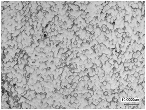
The invention discloses an additive for acid polishing of a silicon wafer. The additive comprises the following components in parts by mass: 0.5 to 1.5 parts of polyaspartic acid, 2.0 to 4.5 parts ofacetic acid, 1.0 to 2.0 parts of stachyose, 2.0 to 3.5 parts of sorbitol and 100 parts of water. The additive disclosed by the invention is added into a polishing solution for acid polishing of the silicon wafer, so a suede surface located on the back of the silicon wafer after acid polishing is changed into a tower footing shape.

Description

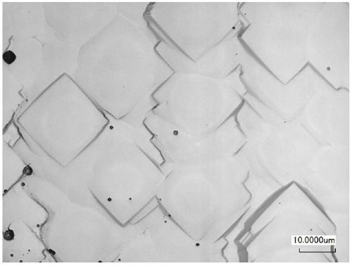
technical field [0001] The invention relates to the field of photovoltaics, in particular to an additive for silicon sheet acid polishing and application thereof. Background technique [0002] Crystalline silicon solar cells generally have to prepare a pyramid-structured texture on the surface of the silicon wafer, and if the pyramid-structured texture is retained on the back of the silicon wafer, various defects will occur. Therefore, in the production process of the cell, the back of the silicon wafer needs to be polished. , that is, back polishing. [0003] At present, the back polishing of silicon wafers mainly includes acid polishing and alkali polishing. [0004] Such as figure 1 As shown, after the back of the silicon wafer is subjected to conventional alkali polishing, the back of the silicon wafer becomes relatively flat, and the suede on the back of the silicon wafer becomes tower-like, that is, after the pyramid structure of the original suede is subjected to al...

Claims


Application Information

Patent Timeline
Patent Type & Authority Applications(China)
IPC IPC(8): C30B33/10C30B29/06C23F1/24
CPCC30B29/06C30B33/10
Inventor 于胤邓舜陈盼盼章圆圆
Owner CHANGZHOU SHICHUANG ENERGY CO LTD
Learn More