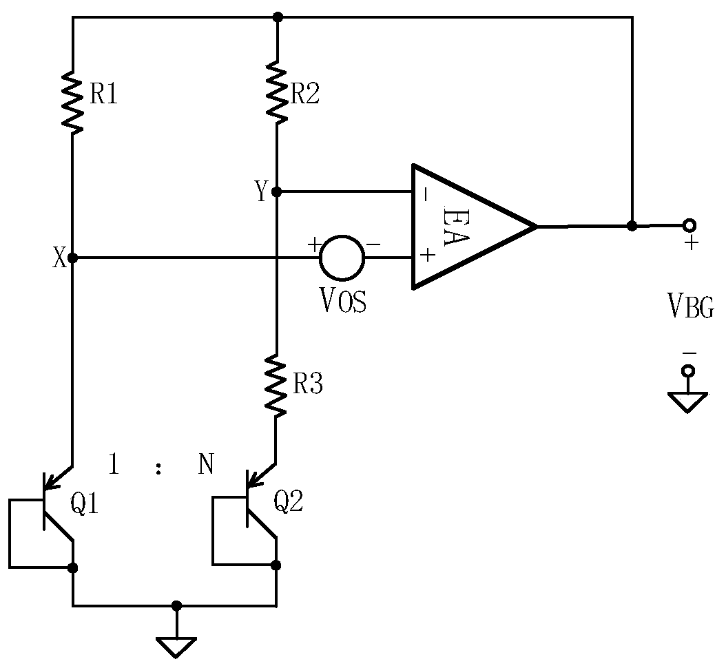
Operational amplifier-free band-gap reference circuit with pre-voltage-stabilizing structure
A reference circuit and pre-regulation technology, applied in the field of circuits, can solve the problems of difficulty in meeting the requirements of the power supply rejection ratio, low power supply rejection ratio of the circuit, and increase of circuit power consumption, so as to weaken the influence of accuracy and improve the power supply rejection. ratio, the effect of reducing circuit power consumption
- Summary
- Abstract
- Description
- Claims
- Application Information
AI Technical Summary
Problems solved by technology
Method used
Image
Examples
Embodiment 1
[0030] refer to figure 2 , the present invention includes: a bandgap core unit 1, an output unit 2, a pre-stabilizing unit 3 and a starting unit 4; wherein the bandgap core unit 1 is provided with two input terminals, respectively connected to the reference voltage V BG and the premodulation voltage V REG , with an output output feedback voltage V FB ; The output unit 2 has an input terminal connected to the premodulation voltage V REG , with two output terminals, which respectively output the bandgap voltage V BG and zero temperature coefficient voltage V O ; The pre-stabilizing unit 3 is provided with two input terminals, respectively connected to the feedback voltage V FB and the start signal Vstart, with two output terminals, which respectively output the pre-regulated voltage V REG and bias voltage V BIAS ; The starting unit 4 is provided with an input terminal connected to the bias voltage V BIAS , and an output end is provided to output a start signal Vstart.
...
Embodiment 2
[0062] The bandgap core unit 1 and the starting unit 3 of the present invention are the same as those in the first embodiment.
[0063] refer to Figure 4 , the above output unit 2 includes a PMOS transistor MP9 and two resistors R4, R5; wherein: the ninth PMOS transistor MP9, its source is connected to the output V of the pre-regulator unit 3 REG , whose gate is connected to its own source and connected to one end of the fifth resistor R5 as the output V of the entire bandgap reference circuit O ; The fourth resistance R4, one end of which is connected with the other end of the fifth resistance R5, as the output V of the whole bandgap reference circuit BG , the other end of which is connected to GND.
[0064] Output cell 2 is preregulated by the voltage V REG power supply, the current I flowing through the ninth PMOS transistor MP9 MP9 for:
[0065]
[0066] The current I can be adjusted by adjusting the resistance value of the fourth resistor R4 MP9 At the same time...
PUM
 Abstract
Description
Claims
Application Information
 - R&D Engineer
- R&D Manager
- IP Professional
- Industry Leading Data Capabilities
- Powerful AI technology
- Patent DNA Extraction
Browse by: Latest US Patents, China's latest patents, Technical Efficacy Thesaurus, Application Domain, Technology Topic, Popular Technical Reports.
© 2024 PatSnap. All rights reserved.Legal|Privacy policy|Modern Slavery Act Transparency Statement|Sitemap|About US| Contact US: help@patsnap.com


