Perovskite 2D/3D LED structure and preparation method thereof

A 3D LED and perovskite technology, applied in the field of preparation of new electronic components, can solve the problems of inability to protect materials from moisture and oxygen erosion, and achieve improved water stability, high turn-on voltage, and hole extraction promotion Effect

Active Publication Date: 2020-05-22
DALIAN UNIV OF TECH
View PDF6 Cites 0 Cited by
  • Summary
  • Abstract
  • Description
  • Claims
  • Application Information

AI Technical Summary

Problems solved by technology

However, there are still limitations in using these passivators as post-synthetic perovskite treatments to improve efficiency and stability.
The secondary bonds between these passivating molecules and the perovskite surface are usually too weak to protect the material from moisture and oxygen.
Not all structural defects are electronic defects, so some structural defects that may lead to membrane degradation may not be covered by passivating molecules

Method used


Image

  • Perovskite 2D/3D LED structure and preparation method thereof
  • Perovskite 2D/3D LED structure and preparation method thereof
  • Perovskite 2D/3D LED structure and preparation method thereof

Examples


Embodiment Construction

[0025] The present invention will be further described below in conjunction with specific drawings and embodiments.

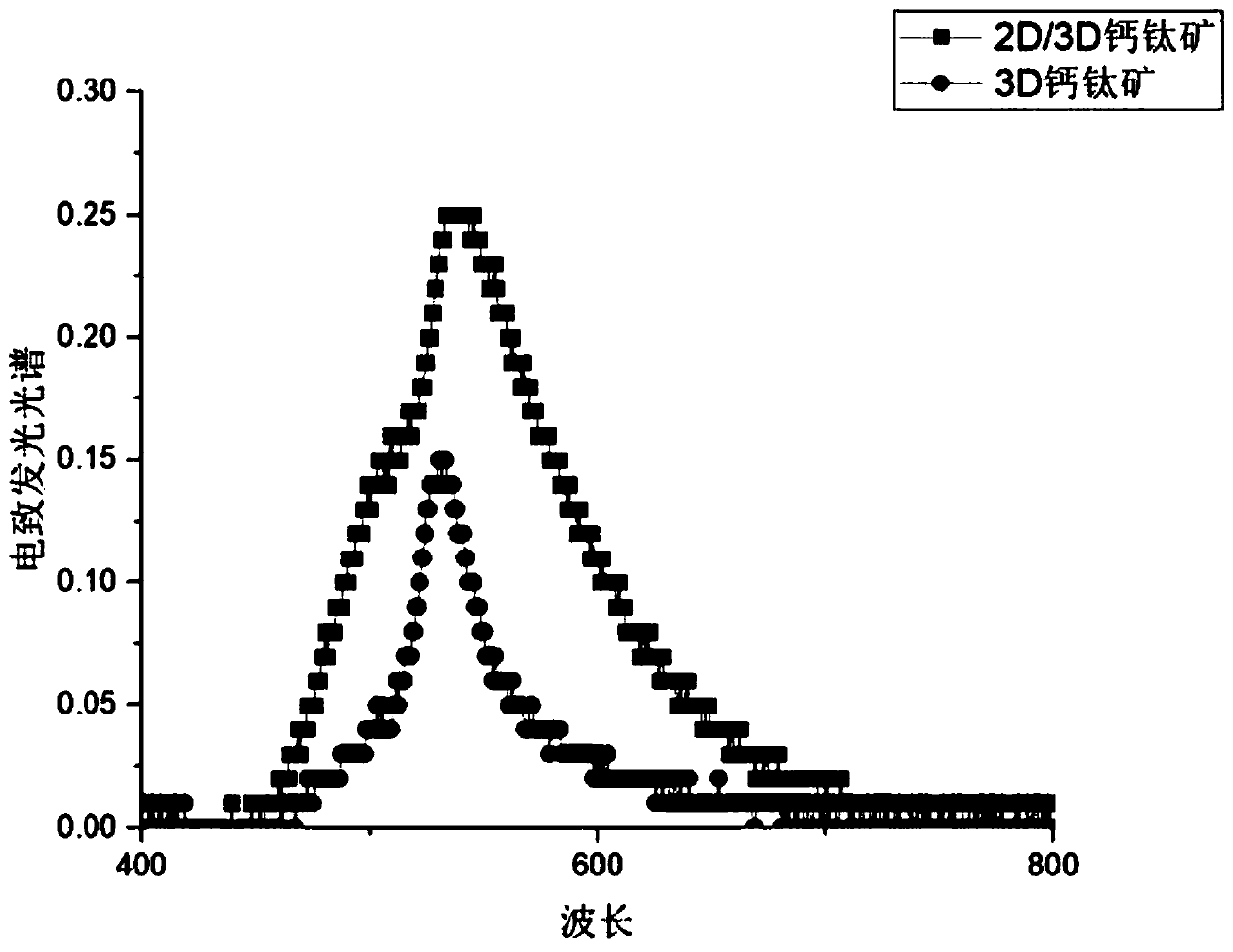
[0026] A perovskite 2D / 3D LED structure of the present invention includes a multi-layer structure, which is a hole transport layer, a light-emitting layer, an electron transport layer and an electrode from bottom to top. The structure is as follows figure 1 As shown, in this embodiment, the electrodes are gold electrodes.

[0027] A kind of preparation method of perovskite 2D / 3D LED structure of the present invention is as follows (wherein, relate to spin-coating process in each step, such as Figure 4 shown):

[0028] Step 1, cleaning the transparent conductive glass substrate, the substrate used is etched ITO glass

[0029] Using transparent and conductive ITO glass as the substrate, it is chemically cleaned. The cleaning steps are: first, the substrate is ultrasonically oscillated with detergent and deionized water for 10 minutes, and then deionized water,...


PUM

PropertyMeasurementUnit
Thicknessaaaaaaaaaa
Thicknessaaaaaaaaaa
Thicknessaaaaaaaaaa

Abstract

The invention belongs to the field of preparation of novel electronic components, and particularly relates to a perovskite 2D / 3D LED structure and a preparation method thereof. According to the invention, the moisture stability of unsealed films and devices of the LED under high humidity is obviously improved; the 2D covering layer causes greater Fermi level splitting in the 2D-3D perovskite thinfilm, resulting in higher turn-on voltage: in the 2D-3D perovskite device, hole extraction is also promoted, and energy band arrangement and non-radiative recombination in a sub-energy gap state are reduced. The perovskite 2D / 3D LED structure is simple and compact in structure, a passivating agent does not need to be additionally added, the advantages of a two-dimensional material and a three-dimensional material are considered, the performance of the perovskite LED can be improved, and meanwhile long-term stability is obtained.

Description

technical field [0001] The invention belongs to the field of preparation of novel electronic components, and in particular relates to a perovskite 2D / 3D LED structure and a preparation method. Background technique [0002] In recent years, halide perovskite ABX 3 (A=organic cation or metal cation, B=metal cation, X=halogen anion) have excellent optoelectronic properties, including tunable direct bandgap, excellent carrier transport characteristics, and high photoelectric conversion efficiency. Perovskite-based light-emitting diodes have the advantages of good color purity and easy processing, which can meet the needs of the display market. For example, light-emitting diodes (LEDs) based on these materials may find applications in flat-panel displays and solid-state lighting, as they have the potential to be fabricated at low cost through convenient solution processing and can offer tunable colors and narrow emission-line highlights The width under the luminescence quantum ...

Claims


Application Information

Patent Timeline
IPC IPC(8): H01L51/50H01L51/54H01L51/56
CPCH10K85/30H10K50/13H10K71/00
Inventor 毕胜李钰孙业青卜镜元
Owner DALIAN UNIV OF TECH
Why Eureka
Try Eureka