Program on-orbit loading refreshing method based on triple modular redundancy
A three-mode redundancy and program technology, applied in the field of satellite payloads, can solve the problems of inability to modify and high cost of PROM devices, and achieve the effect of shortening the research and development cycle, saving hardware costs, and ensuring correctness.
- Summary
- Abstract
- Description
- Claims
- Application Information
AI Technical Summary
Problems solved by technology
Method used
Image
Examples
Embodiment 1
[0066] A method for on-orbit loading and refreshing of programs based on triple-mode redundancy, the implementation steps are as follows:
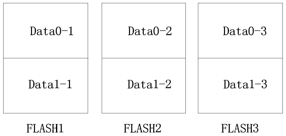
[0067] (1) Prepare three FLASH chips, such as figure 1 As shown, each FLASH chip is divided into two areas according to the address, as the main and backup configuration program storage area, respectively the main storage area and the backup storage area, that is, the areas of the three FLASH chips are respectively Data0-1, Data1-1 , Data0-2, Data1-2, Data0-3, Data1-3;
[0068] (2) The configuration program of the SRAM type FPGA and the configuration program of the DSP chip are spliced, arranged in the order that the configuration program of the SRAM type FPGA is in front and the configuration program of the DSP is in the back, and the configuration programs after splicing are written into Data0 respectively -1, Data0-2, Data0-3, store the backup version of the spliced configuration program in Data1-1, Data1-2, Data1-3;
[0069] (3) Us...
Embodiment 2
[0081] A method for on-orbit loading and refreshing of programs based on triple-mode redundancy, the implementation steps are as follows:
[0082] (1) Prepare three FLASH chips, such as figure 1 As shown, each FLASH chip is divided into two areas according to the address, as the main and backup configuration program storage area, respectively the main storage area and the backup storage area, that is, the areas of the three FLASH chips are respectively Data0-1, Data1-1 , Data0-2, Data1-2, Data0-3, Data1-3;
[0083] (2) The configuration program of the SRAM type FPGA and the configuration program of the DSP chip are spliced, arranged in the order that the configuration program of the SRAM type FPGA is in front and the configuration program of the DSP is in the back, and the configuration programs after splicing are written into Data0 respectively -1, Data0-2, Data0-3, store the backup version of the spliced configuration program in Data1-1, Data1-2, Data1-3;
[0084] (3) Us...
PUM
 Abstract
Description
Claims
Application Information
 - R&D
- Intellectual Property
- Life Sciences
- Materials
- Tech Scout
- Unparalleled Data Quality
- Higher Quality Content
- 60% Fewer Hallucinations
Browse by: Latest US Patents, China's latest patents, Technical Efficacy Thesaurus, Application Domain, Technology Topic, Popular Technical Reports.
© 2025 PatSnap. All rights reserved.Legal|Privacy policy|Modern Slavery Act Transparency Statement|Sitemap|About US| Contact US: help@patsnap.com


