Repairing device of display panel

A technology for display panels and accommodating cavities, which can be applied to identification devices, transportation and packaging, instruments, etc., which can solve problems such as long working hours and complicated manufacturing processes, and achieve the effects of shortening working hours and simplifying the repair process

Inactive Publication Date: 2020-05-15
TCL CHINA STAR OPTOELECTRONICS TECH CO LTD
View PDF9 Cites 1 Cited by
  • Summary
  • Abstract
  • Description
  • Claims
  • Application Information

AI Technical Summary

Problems solved by technology

In the repair process, different process fixtures need to be prepared for substrates with different pixel specifications, resulting in complex process and long working hours.

Method used


Image

  • Repairing device of display panel
  • Repairing device of display panel
  • Repairing device of display panel

Examples


Embodiment Construction

[0025] The following will clearly and completely describe the technical solution in the application with reference to the accompanying drawings in the implementation manner of the application. Apparently, the described implementations are only some of the implementations of this application, not all of them. Based on the implementation manners in this application, all other implementation manners obtained by those skilled in the art without creative efforts shall fall within the scope of protection of this application.

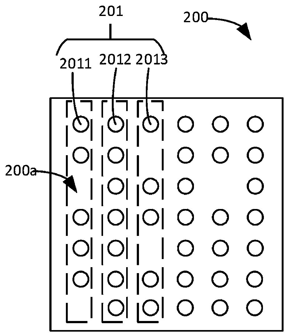
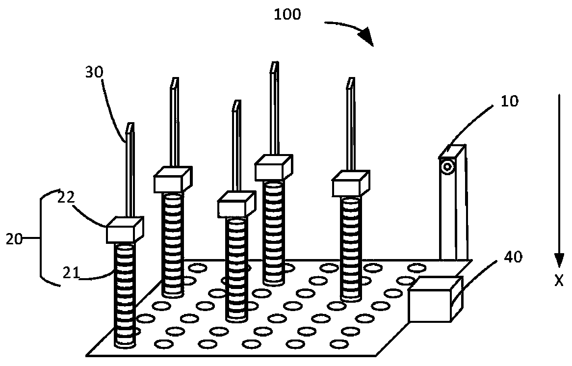
[0026] Please refer to figure 1 and figure 2 , the first embodiment of the present application provides a display panel repairing device 100, which is used for defect repairing of a display panel 200 having a defect 200a. The display panel 200 is a Micro Light-Emitting Diode (Micro LED) display panel. The display panel 200 includes a plurality of light emitting chips 201 . A plurality of light emitting chips 201 are arranged in an array. The light emitti...


PUM


Abstract

The invention provides a repairing device of a display panel, and the device comprises a defect sensor which is used for carrying out the defect inspection of the display panel, and obtaining defect information; a chip picking and placing part which is used for picking up, storing and releasing the light-emitting chips, wherein the chip taking and placing part comprises a chip accommodating cavityand a controller, the chip accommodating cavity is used for storing the light-emitting chips, and the controller is used for picking up and releasing the chips; a chip moving part which is connectedwith the chip taking and placing part and is used for moving the chip taking and placing part to the position of the defect according to the defect information; and a chip binding part which is used for binding the light-emitting chip on the display panel.

Description

technical field [0001] The present application relates to the display field, in particular to a repairing device for a display panel. Background technique [0002] Micro-light emitting diodes (Micro-light emitting diodes, MicroLED) have the advantages of high brightness, good luminous efficiency, low power consumption, long life and thinness. It is expected to become the mainstream display technology of the next generation. [0003] The manufacturing method of Micro LED is mainly to arrange arrays of LEDs of several microns to tens of microns after miniaturization on the substrate to form an LED array with high density and small size. However, the lighting yield of Micro LED display devices manufactured by mass transfer still cannot meet the technical requirements of 99.9999% in the mass production stage. Therefore, the display panel needs to be repaired after the transfer process is completed. In the repair process, different process fixtures need to be prepared for subs...

Claims


Application Information

Patent Timeline
Patent Type & Authority Applications(China)
IPC IPC(8): H01L21/66H01L21/677H01L21/683H01L33/62G09F9/33
CPCH01L22/12H01L22/20H01L21/6835H01L33/62G09F9/33H01L21/67763H01L2933/0066H01L2221/68313H01L33/0095H01L25/0753H01L25/167H01L21/67288H01L21/67144H01L21/6831H01L21/6838
Inventor 张玮柳铭岗孙洋陈书志
Owner TCL CHINA STAR OPTOELECTRONICS TECH CO LTD
Why Eureka
Try Eureka