
Spliced printed circuit substrate structure

A printed circuit substrate and splicing technology, which is applied to the structural connection of printed circuits, printed circuits, printed circuit components, etc. Stability of splicing, not easy to fall off and loose, and the effect of accelerating heat dissipation

Inactive Publication Date: 2020-05-08
JIANGXI UNIV OF TECH
View PDF20 Cites 2 Cited by
  • Summary
  • Abstract
  • Description
  • Claims
  • Application Information

AI Technical Summary

Problems solved by technology

[0003] However, the existing substrate structure is not easy to splice and cannot meet the actual needs of use. Moreover, the existing substrate structure is not easy to dissipate heat, and its internal components are easily damaged by high temperature.

Method used


Image

  • Spliced printed circuit substrate structure
  • Spliced printed circuit substrate structure
  • Spliced printed circuit substrate structure

Examples


Embodiment Construction

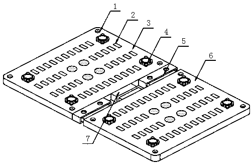
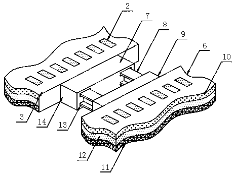
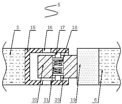
[0020] See Figure 1~4 In the embodiment of the present invention, a spliced ​​printed circuit substrate structure includes a first substrate 3 and a second substrate 6 located on one side of the first substrate 3. The upper surface corners of the first substrate 3 and the second substrate 6 are both A first screw hole 1 is opened, and the inside of the first substrate 3 and the second substrate 6 are sequentially bonded with a base material layer 11, a circuit layer 12 and an insulating layer 10 from the inside to the outside, the first substrate 3 and the second substrate 6 LED chips 2 are embedded and mounted on the upper surfaces of the first substrate 3 and the second substrate 6 are embedded and mounted on the upper surface edges of the heat dissipation assembly 4, the heat dissipation assembly 4 includes a first heat sink 23, a first heat dissipation fin 24, heat The rod 25, the mounting rod 26, the second heat sink 27 and the second heat dissipation fin 28. The top end ...


PUM


Abstract

The invention relates to the technical field of printed circuit substrates, and discloses a spliced printed circuit substrate structure. First screw holes are formed in the corners of the upper surfaces of a first substrate and a second substrate correspondingly. A base material layer, a circuit layer and an insulating layer are sequentially adhered to the interiors of the first substrate and thesecond substrate from inside to outside; heat dissipation assemblies are embedded in the edges of the upper surfaces of the first substrate and the second substrate correspondingly, a connecting assembly is further connected between the first substrate and the second substrate, and clamping assemblies are connected to the positions, close to the two sides of the connecting assembly, between the first substrate and the second substrate correspondingly. The clamping assembly and the connecting assembly are combined for use; by means of the clamping assembly, a user can conveniently splice the first substrate and the second substrate and conveniently use the first substrate and the second substrate according to actual use requirements, the splicing stability between the first substrate and the second substrate can be improved through the clamping assembly, and the first substrate and the second substrate are not prone to falling off or loosening after being spliced.

Description

Technical field [0001] The invention relates to the technical field of printed circuit substrates, in particular to a spliced ​​printed circuit substrate structure. Background technique [0002] Circuit printing adopts photo-engraving technology, that is, the base plate of the photographed picture is etched on a copper plate or a zinc plate. This type of copper plate or zinc plate is used for printing, which has made significant progress compared with the traditional circuit board, and the substrate is made of PCB. The basic material, under normal circumstances, the substrate is a copper clad laminate. Single and double-sided printed boards are manufactured on the substrate material-copper clad laminate, with selective hole processing, electroless copper plating, and copper electroplating , Etching and other processing to obtain the required circuit pattern. [0003] However, the existing substrate structure is not easy to splice and cannot meet actual use needs. Moreover, the exi...

Claims


Application Information

Patent Timeline
Patent Type & Authority Applications(China)
IPC IPC(8): H05K1/02H05K1/14
CPCH05K1/0209H05K1/021H05K1/14
Inventor 徐飞龙
Owner JIANGXI UNIV OF TECH
Learn More