Through-silicon via (TSV) interconnection structure and preparation method thereof

A technology of interconnection structure and through-silicon via, which is applied in semiconductor/solid-state device manufacturing, semiconductor/solid-state device components, semiconductor devices, etc., can solve the problems of time-consuming, high cost, and low yield.

Pending Publication Date: 2020-05-05
CHANGXIN MEMORY TECH INC
View PDF0 Cites 0 Cited by
  • Summary
  • Abstract
  • Description
  • Claims
  • Application Information

AI Technical Summary

Problems solved by technology

[0007] The purpose of the present invention is to overcome the shortcomings of the above-mentioned prior art that it takes too long to manufacture, the cost is too high, and the yield rate is low, and to provide a through-silicon via interconnection structure with better benignity, which can reduce production time-consuming and production costs. its preparation method

Method used


Image

  • Through-silicon via (TSV) interconnection structure and preparation method thereof
  • Through-silicon via (TSV) interconnection structure and preparation method thereof
  • Through-silicon via (TSV) interconnection structure and preparation method thereof

Examples


Embodiment Construction

[0060] Example embodiments will now be described more fully with reference to the accompanying drawings. Example embodiments may, however, be embodied in many forms and should not be construed as limited to the embodiments set forth herein; rather, these embodiments are provided so that this disclosure will be thorough and complete, and will fully convey the concept of example embodiments to those skilled in the art. The same reference numerals in the drawings denote the same or similar structures, and thus their detailed descriptions will be omitted.

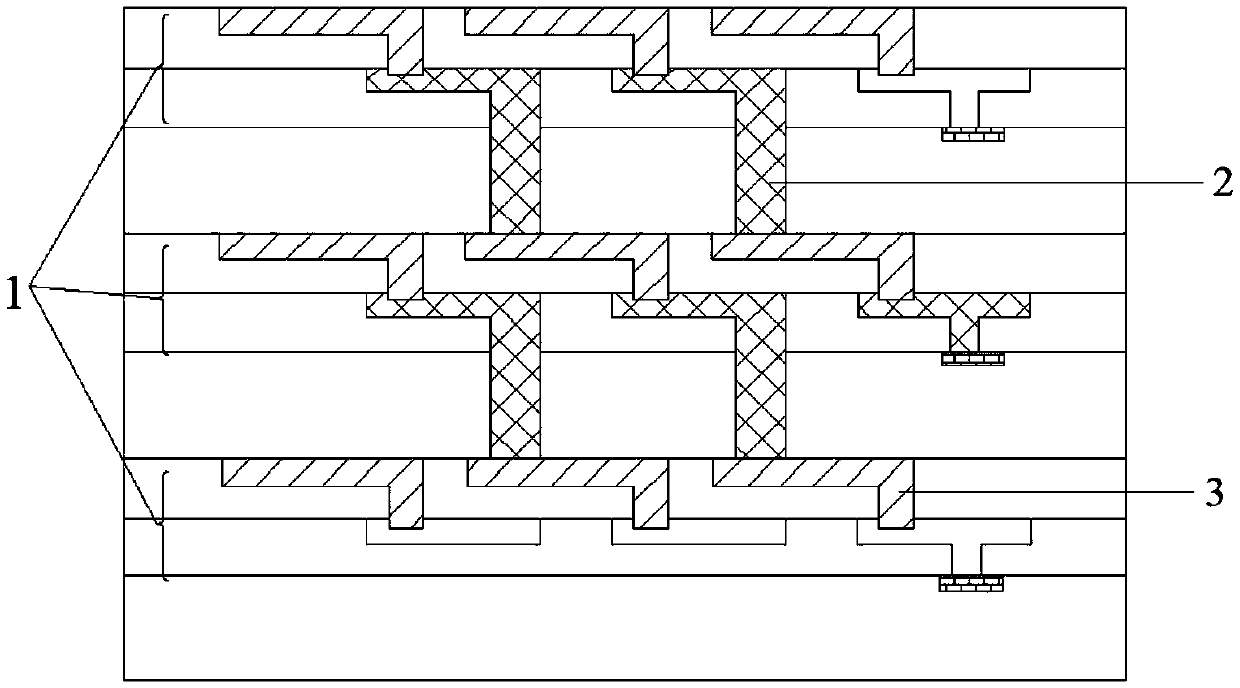
[0061] refer to figure 1 The schematic diagram of the TSV interconnection structure in the related art is shown. In the related art, the displacement of the TSV is formed by wire winding, which generally requires RDL (redistribution layer 1) to achieve, the manufacturing process is relatively complicated, and the time required is also short. There are more, and the cost is higher and the yield is lower.

[0062] The present ...


PUM


Abstract

The invention relates to the technical field of semiconductors, and provides a through-silicon via (TSV) interconnection structure and a preparation method thereof. The through-silicon via (TSV) interconnection structure can comprise multiple layers of substrates and connecting wires. Each layer of substrate of the multiple layers of substrates is provided with a plurality of through-silicon vias,and the layers of substrates are sequentially stacked in a staggered manner to make the through-silicon vias partially communicated; and the connecting wires are arranged in the through-silicon viasto connect corresponding circuits on the multiple layers of substrates. According to the invention, the staggered arrangement of the substrates is utilized, so that the through silicon vias on each layer of substrate are connected in a staggered manner to meet the requirements of through silicon vias (TSV) jumper without using a RDL; and the TSV interconnection structure is good in yield, and theproduction time consumption and the production cost can be reduced.

Description

technical field [0001] The invention relates to the technical field of semiconductors, in particular to a through-silicon via interconnection structure and a preparation method thereof. Background technique [0002] TSVThrough Silicon Vias (TSVThrough Silicon Vias) are often used when saving valuable layout space or increasing the efficiency of interconnects. A TSV is a vertical conductive via that can completely penetrate a substrate or wafer made of silicon material. [0003] The TSV displacement in the prior art is formed by winding metal wires, which is generally achieved by using RDL (Re-Distribution Layer). [0004] However, its manufacturing process is too complicated, it takes too long to make, the cost is too high, and the yield rate is low. [0005] Therefore, it is necessary to study a new TSV interconnection structure and its preparation method. [0006] The above information in this Background section is only for enhancement of understanding of the background...

Claims


Application Information

Patent Timeline
Patent Type & Authority Applications(China)
IPC IPC(8): H01L23/48H01L23/528H01L21/768
CPCH01L23/481H01L23/5283H01L21/76898H01L2224/08145
Inventor 不公告发明人
Owner CHANGXIN MEMORY TECH INC
Why Eureka
Try Eureka