A device and method for two-dimensional imaging based on single photon counting

A single-photon counting and single-photon counter technology, applied in the direction of instruments, can solve the problems of inability to realize quantum tomography and low resolution, and achieve low resolution and inability to accurately image, stable scanning and detection, and convenient optical intervention Effect

Active Publication Date: 2021-02-12
TAIYUAN UNIV OF TECH
View PDF8 Cites 0 Cited by
  • Summary
  • Abstract
  • Description
  • Claims
  • Application Information

AI Technical Summary

Problems solved by technology

[0004] In order to solve the problems of low resolution and inability to realize quantum tomography in existing common imaging devices, the present invention provides a high-precision and high-resolution two-dimensional imaging device and method based on single photon counting

Method used


Image

  • A device and method for two-dimensional imaging based on single photon counting
  • A device and method for two-dimensional imaging based on single photon counting
  • A device and method for two-dimensional imaging based on single photon counting

Examples


Embodiment Construction

[0034] In order to make the purpose, technical solutions and advantages of the embodiments of the present invention clearer, the technical solutions in the embodiments of the present invention will be clearly and completely described below. Obviously, the described embodiments are part of the embodiments of the present invention, rather than All the embodiments; based on the embodiments of the present invention, all other embodiments obtained by persons of ordinary skill in the art without creative work all belong to the protection scope of the present invention.

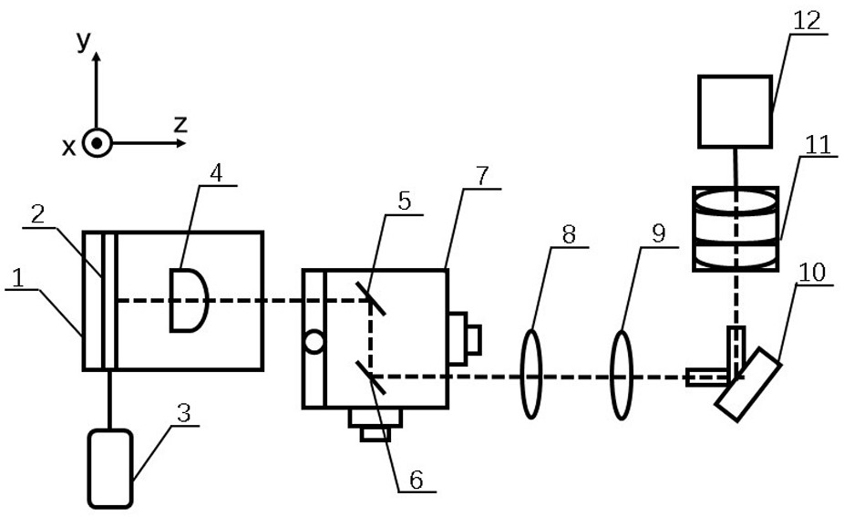
[0035] Such as figure 1 As shown, the embodiment of the present invention provides a device based on single-photon counting two-dimensional imaging, including a vacuum chamber 1, an aspheric mirror 4, a laser 3, a displacement platform 7, a collimation device, a high-speed scanning galvanometer 10, a coupling 11, a single photon counter 12, a data acquisition card and a computing unit (not shown in the figure).

[...


PUM

PropertyMeasurementUnit
particle sizeaaaaaaaaaa
wavelengthaaaaaaaaaa

Abstract

The invention relates to the field of nano-imaging. In order to solve the problem of imaging nano-fiber size devices, a device for two-dimensional imaging using single photon counting is disclosed, including a vacuum chamber, an aspheric mirror, a laser, a displacement platform, and a collimator. device, high-speed scanning galvanometer, coupler, single photon counter, data acquisition card and computing unit; the laser light emitted by the laser is transmitted to the nano-fiber to be tested in the vacuum chamber through a single-mode fiber and then scattered, and the scattered light signal collected by the aspheric mirror After passing through the first and second 45-degree mirrors, collimation device and high-speed scanning galvanometer, it is incident on the single photon counter through the coupler, and the data acquisition card is used to collect the electrical signal obtained by the photoelectric conversion of the single photon counter and send it to computing unit. The invention uses single photon counting to obtain optical fiber two-dimensional imaging, has high imaging precision and good image restoration, and can be widely used in the field of two-dimensional imaging of optical transmission media with a size of hundreds of nanometers.

Description

technical field [0001] The invention relates to the field of nanometer imaging, in particular to a device and method for two-dimensional imaging based on single photon counting. Background technique [0002] At present, there are transmission electron microscopy, scanning tunneling microscopy, atomic force microscopy and other techniques for the detection and characterization of nanomaterials. For example, a high-resolution scanning electron microscope can scan and image barium titanate ceramics with a grain size of 20 nm. However, the high-resolution scanning electron microscope can only obtain the morphology observation or size detection of nano-scale materials, and cannot obtain the overall structural information of larger-sized objects without loss. In addition, the developed fluorescence imaging system can achieve a spatial resolution of tens of nanometers, but due to the autofluorescence phenomenon of the object and the residual excitation light signal, there is a lar...

Claims


Application Information

Patent Timeline
Patent Type & Authority Patents(China)
IPC IPC(8): G01J11/00
CPCG01J11/00
Inventor 郭龑强张浩杰郭晓敏赵彤
Owner TAIYUAN UNIV OF TECH
Why Eureka
Try Eureka