A kind of semiconductor laser and its preparation method

A laser and semiconductor technology, applied in the field of optoelectronics, which can solve the problems of poor beam quality and low laser brightness.

Active Publication Date: 2021-10-08
CHANGCHUN INST OF OPTICS FINE MECHANICS & PHYSICS CHINESE ACAD OF SCI
View PDF5 Cites 0 Cited by
  • Summary
  • Abstract
  • Description
  • Claims
  • Application Information

AI Technical Summary

Problems solved by technology

[0003] At present, high-power semiconductor lasers usually adopt a wide-area structure in the lateral direction. Affected by effects such as thermal lens, carrier accumulation at the edge of the mesa, and photocarrier anti-guiding, the laser works in a complex multi-mode mode laterally, and the beam quality Very poor, resulting in the rapid increase of the lateral far field of the laser with the increase of the operating current, and the output laser brightness is very low

Method used


Image

  • A kind of semiconductor laser and its preparation method
  • A kind of semiconductor laser and its preparation method
  • A kind of semiconductor laser and its preparation method

Examples


Embodiment Construction

[0029] The following will clearly and completely describe the technical solutions in the embodiments of the application with reference to the drawings in the embodiments of the application. Apparently, the described embodiments are only some of the embodiments of the application, not all of them. Based on the embodiments in this application, all other embodiments obtained by persons of ordinary skill in the art without making creative efforts belong to the scope of protection of this application.

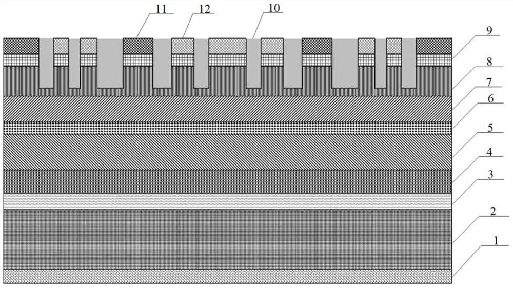
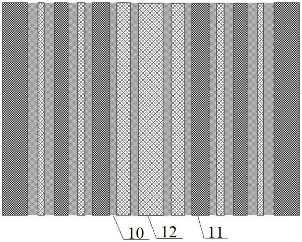
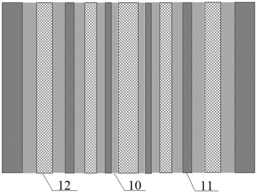
[0030] see figure 1 , which shows a schematic structural diagram of a semiconductor laser provided in an embodiment of the present application. A semiconductor laser provided in an embodiment of the present application may sequentially include an N-face electrode 1, a substrate 2, a buffer layer 3, a N Type cladding layer 4, N-plane waveguide 5, active region 6, P-plane waveguide 7, P-type cladding layer 8, P-type cladding layer 9, P-type cladding layer 9 and P-type cladding layer 8...


PUM

PropertyMeasurementUnit
widthaaaaaaaaaa
widthaaaaaaaaaa

Abstract

The application discloses a semiconductor laser and its preparation method. The semiconductor laser includes an N-face electrode, a substrate, a buffer layer, an N-type cladding layer, an N-face waveguide, an active region, a P-face waveguide, and a P-type cladding layer from bottom to top. , P-type capping layer, the P-type capping layer and the P-type cladding layer with a preset thickness form multiple ridge-shaped strips, and the adjacent two ridge-shaped strips are separated by insulating isolation trenches; The surface of the ridge strips outside the peak of the light field and located at the peak of the light field of the high-order side mode is covered with an electrical insulating layer, and the surface of the remaining ridge strips is covered with a P-plane electrode. In the above-mentioned technical scheme disclosed in the present application, an electrical insulating layer is arranged on the ridge-shaped strip at the peak of the light field of the high-order side mode, and a P-face electrode is arranged on the remaining ridge-shaped strip, so as to pass through the electric insulating layer and the P-face electrode when energized. Selective power-on is achieved, thereby increasing the optical loss of the high-order side mode and reducing the gain of the high-order side mode, so as to reduce the number of lasing side modes, thereby improving the quality and brightness of the laser beam.

Description

technical field [0001] The present application relates to the field of optoelectronic technology, and more specifically, to a semiconductor laser and a preparation method thereof. Background technique [0002] Semiconductor lasers have the characteristics of small size, high efficiency, and long life, so they have very wide applications. With the expansion of the application market of semiconductor lasers, the brightness requirements of semiconductor lasers are getting higher and higher in the fields of fiber laser pumping, display, frequency conversion, material processing, laser radar, medical and national defense, etc., which requires semiconductor lasers to have high output power and high beam quality. [0003] At present, high-power semiconductor lasers usually adopt a wide-area structure in the lateral direction. Affected by effects such as thermal lens, carrier accumulation at the edge of the mesa, and photocarrier anti-guiding, the laser works in a complex multi-mod...

Claims


Application Information

Patent Timeline
Patent Type & Authority Patents(China)
IPC IPC(8): H01S5/068H01S5/10
CPCH01S5/068H01S5/1039H01S5/1082
Inventor 汪丽杰佟存柱舒世立田思聪张新陆寰宇王延靖宿家鑫
Owner CHANGCHUN INST OF OPTICS FINE MECHANICS & PHYSICS CHINESE ACAD OF SCI
Why Eureka
Try Eureka