Vanadium dioxide intelligent thermal control device with longhorn beetle-imitating multistage structure and preparation method thereof
A technology of vanadium dioxide intelligence and longhorn, which is applied in the control of the living conditions of aerospace vehicles, ion implantation plating, coating, etc., can solve the problems of small emissivity change and high solar absorption ratio
- Summary
- Abstract
- Description
- Claims
- Application Information
AI Technical Summary
Problems solved by technology
Method used
Image
Examples
specific Embodiment approach 1
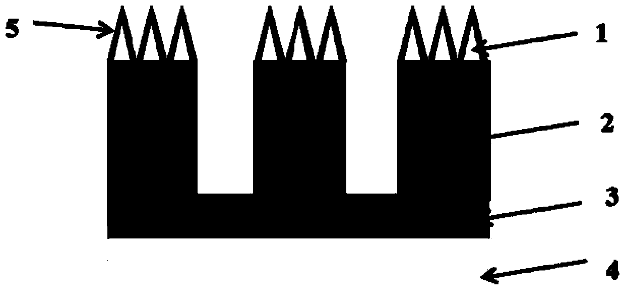
[0027] Specific implementation mode one: combine figure 1 Describe this embodiment in detail. In this embodiment, a vanadium dioxide intelligent thermal control device with a multi-level structure imitating a beetle is sequentially composed of a semiconductor base layer, an infrared highly reflective metal layer, HfO 2 Dielectric layer, VO 2 layer and protective layer composition;
[0028] The HfO 2 The dielectric layer consists of multiple HfO 2 Composed of micro-nano structural units, and HfO 2 The shape of the micro-nano structural unit is a cube with a square base, and multiple HfO 2 The micro-nano structural units are uniformly arranged on the upper surface of the infrared highly reflective metal layer; the HfO 2 The bottom square of the micro-nano structural unit has a side length of 1 μm to 10 μm and a height of 400nm to 2000nm; adjacent HfO 2 The distance between micro-nano structural units is 0.5 μm to 5 μm;
[0029] The VO 2 layer consists of multiple W-doped...
specific Embodiment approach 2
[0033] Embodiment 2: This embodiment is different from Embodiment 1 in that: the semiconductor base layer is quartz, glass or silicon; the infrared highly reflective metal layer is Ag, Ni, Mg, Zn or Al; The above protective layer is Al 2 o 3 , SiO 2 、TiO 2 or ZrO 2 . Others are the same as in the first embodiment.
specific Embodiment approach 3
[0034] Specific embodiment three: the difference between this embodiment and specific embodiment one or two is that: the thickness of the infrared highly reflective metal layer is 50nm-250nm; the HfO 2 The thickness of the dielectric layer is 400nm-2000nm; the VO 2 The thickness of the layer is 50nm-500nm; the thickness of the protective layer is 50nm-100nm. Others are the same as those in the first or second embodiment.
PUM
| Property | Measurement | Unit |
|---|---|---|
| Side length | aaaaa | aaaaa |
| Height | aaaaa | aaaaa |
| Bottom diameter | aaaaa | aaaaa |
Abstract
Description
Claims
Application Information
 - R&D
- Intellectual Property
- Life Sciences
- Materials
- Tech Scout
- Unparalleled Data Quality
- Higher Quality Content
- 60% Fewer Hallucinations
Browse by: Latest US Patents, China's latest patents, Technical Efficacy Thesaurus, Application Domain, Technology Topic, Popular Technical Reports.
© 2025 PatSnap. All rights reserved.Legal|Privacy policy|Modern Slavery Act Transparency Statement|Sitemap|About US| Contact US: help@patsnap.com

