A method for fast tin conduction of multi-layer interconnected FPC

A fast and conductive technology, applied in the direction of electrical components, printed circuit manufacturing, printed circuit, etc., can solve the problem of pad size limitation, not being well solved, etc.

Active Publication Date: 2021-04-20
UNIV OF ELECTRONICS SCI & TECH OF CHINA +1
View PDF7 Cites 0 Cited by
  • Summary
  • Abstract
  • Description
  • Claims
  • Application Information

AI Technical Summary

Problems solved by technology

Due to the limited area design of the circuit board, the size of the pads of the main FPC and the auxiliary FPC is limited. To ensure good contact between the main FPC and the auxiliary FPC, it is necessary to ensure that the main FPC and the auxiliary FPC are under the limited pad area. There is a sufficient amount of solder between the pads of the FPC and the auxiliary FPC, but the problem of how to quickly melt enough solder between the pads of the main FPC and the auxiliary FPC is not well obtained in the prior art the solution

Method used


Image

  • A method for fast tin conduction of multi-layer interconnected FPC
  • A method for fast tin conduction of multi-layer interconnected FPC
  • A method for fast tin conduction of multi-layer interconnected FPC

Examples


Embodiment Construction

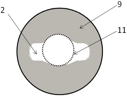
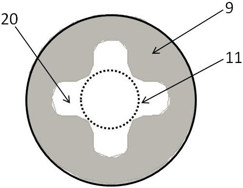
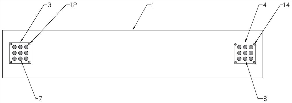
[0021] like Figure 1 to Figure 6 As shown, in this embodiment, a multilayer interconnection FPC realizes a method for fast tin conduction, the multilayer interconnection FPC applied to the method includes a main FPC1 and an auxiliary FPC2, and the main FPC1 is provided with a main output area 3 and a Main input area 4, said auxiliary FPC2 is provided with auxiliary output area 5 and auxiliary input area 6; said main output area 3 is provided with several main output pads 7 connected with said main FPC1 circuit, said main Several main input pads 8 connected to the main FPC1 circuit are arranged in the input area 4, and several main input pads 8 connected to the auxiliary FPC2 circuit and connected to the main input pad 8 are arranged in the auxiliary output area 5. A corresponding auxiliary output pad 9, the auxiliary input area 6 is provided with several auxiliary input pads 10 connected to the auxiliary FPC2 circuit and corresponding to the main output pad 7 one-to-one, the ...


PUM


Abstract

The invention discloses and provides a multi-layer interconnection FPC with fast tin-conducting via holes, which has a simple structure, high material utilization rate, can quickly melt enough solder during welding, and has stable performance. Described a kind of method that multi-layer interconnection FPC realizes fast lead tin is that described lead tin via hole is arranged on described auxiliary output pad and the central position of described auxiliary input pad, the aperture of described lead tin via hole Set to 100um to 300um, the auxiliary output pad and the auxiliary input pad are both ring-shaped, the ring width of the ring is greater than 100um, and several gaps are set on the edge of the tin-conducting via hole, so There is at least one part of the ring without the notch or at least one part of the ring has a width greater than 100um after removing the notch, solder is melted into the tin guide via hole, and the main input pad and the auxiliary output solder The pads are connected by solder, and the main output pad is connected with the auxiliary input pad by solder. The invention is applied to the technical field of FPC production.

Description

technical field [0001] The invention relates to the technical field of flexible circuit boards, in particular to a method for fast tin conduction of multilayer interconnected FPCs. Background technique [0002] Multi-layer board FPC has multi-layer wiring layers, and an insulating layer is provided between two adjacent wiring layers. Multi-layer circuit boards generally have at least three conductive layers, two of which are on the outer surface, and the remaining layer is synthesized Within an insulating board, the electrical connections between them are usually made through plated through-holes in the cross-section of the board. For some multi-layer FPCs, the number of traces in a certain conductive layer is small, resulting in a small actual use area of ​​this layer, low material utilization rate, and great material waste. For this reason, we have developed a multi-layer interconnected FPC composed of a main FPC large board and multiple auxiliary FPC small boards through...

Claims


Application Information

Patent Timeline
Patent Type & Authority Patents(China)
IPC IPC(8): H05K3/36
CPCH05K3/363
Inventor 向勇胡高强覃逸龙曾产税晓明
Owner UNIV OF ELECTRONICS SCI & TECH OF CHINA
Why Eureka
Try Eureka