Wafer edge contour detection method

A detection method and edge profile technology are applied in the field of wafer edge profile detection, which can solve the problems of incomplete wafer edge information detection and the like

Pending Publication Date: 2020-03-31
北京粤海金半导体技术有限公司
View PDF0 Cites 0 Cited by
  • Summary
  • Abstract
  • Description
  • Claims
  • Application Information

AI Technical Summary

Problems solved by technology

[0007] The object of the present invention is to provide a method for detecting the edge profile of a wafer to solve the problem of incomplete detection of edge information of the wafer

Method used


Image

  • Wafer edge contour detection method
  • Wafer edge contour detection method
  • Wafer edge contour detection method

Examples


Embodiment Construction

[0037] Specific embodiments of the present invention will be described in detail below in conjunction with the accompanying drawings. It should be understood that the specific embodiments described here are only used to illustrate and explain the present invention, and are not intended to limit the present invention.

[0038] The present invention provides a detection method of a wafer edge profile, wherein the detection method comprises:

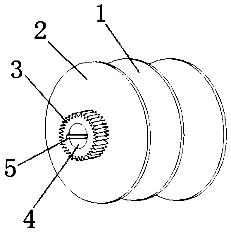
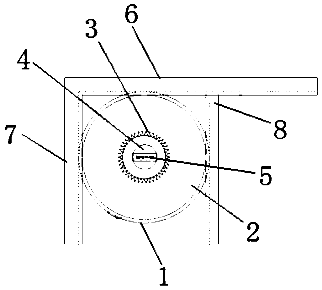
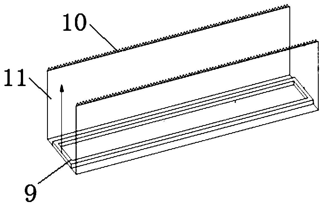
[0039] Step 1, the wafer 1 is clamped on the fixture, and the impression agent is set on the support plate 9;

[0040] Step 2, press the edge of the wafer 1 to be formed into the impression agent, and roll the wafer 1 along a straight line parallel to the support plate 9, and the edge of the wafer 1 to be formed is placed on the die. roll on the agent to form an impression model;

[0041] Step 3, using a laser confocal microscope to continuously scan the impression model successively at different positions along the linear direction, to o...


PUM

PropertyMeasurementUnit
Radial sizeaaaaaaaaaa
Thicknessaaaaaaaaaa

Abstract

The invention relates to the field of wafer detection, and discloses a wafer edge contour detection method. The detection method comprises: the step 1, clamping a wafer (1) on a clamp, and arranging an impression agent on a support disc (9); the step 2, pressing a to-be-formed edge of the wafer (1) into an impression agent, and rolling the wafer (1) to enable the to-be-formed edge of the wafer (1)to roll on the impression agent to form an impression model; the step 3, scanning the model by using a laser confocal microscope to obtain three-dimensional images of the impression model at different positions; and the step 4, splicing the three-dimensional images by using computer software to obtain a three-dimensional edge data model of the wafer (1). According to the technical scheme, the three-dimensional images of the impression model at different positions can be spliced to form the three-dimensional edge data model, and the shape information of the edge can be detected more comprehensively and completely, so that the wafer processing technology can be monitored conveniently, and the wafer production quality can be improved.

Description

technical field [0001] The invention relates to the field of wafer detection, in particular to a method for detecting the edge profile of a wafer. Background technique [0002] There are currently three main methods for detecting the edge profile of a chamfered wafer: [0003] 1. Cut the wafer radially, enlarge it with the help of an optical projector, focus so that the section is clearly projected on the display screen, and compare it with the standard template; [0004] 2. Place the wafer under the parallel optical path, project the edge of the wafer onto the display screen, and compare the image of the edge profile with the coordinate map of the edge profile template; [0005] 3. Place the wafer under the light source, use the CCD camera to display the outline shape image of the edge of the wafer or the notch reference surface on the display screen, and analyze the detection image through the analysis software. [0006] Existing wafer edge detection methods all use proj...

Claims


Application Information

Patent Timeline
IPC IPC(8): G01B11/24G01B5/00
CPCG01B11/24G01B5/00
Inventor 张岩刘振洲王锡铭赵子强赵然陈菲菲
Owner 北京粤海金半导体技术有限公司
Why Eureka
Try Eureka