Multilayer color dynamic display anti-counterfeiting film and preparation method thereof
A technology of dynamic display and film, applied in the field of anti-counterfeiting, can solve the problem of low resolution of dynamic graphics, and achieve the effect of good graphics resolution and obvious display.
- Summary
- Abstract
- Description
- Claims
- Application Information
AI Technical Summary
Problems solved by technology
Method used
Image
Examples
Embodiment 1
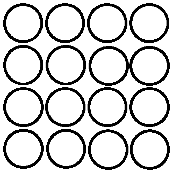
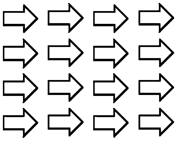
[0036] In this embodiment, the color dynamic display film such as figure 1 As shown, it consists of a microlens array layer, a transparent medium layer I, a transparent medium layer II and a micrographics array metal layer from top to bottom. Among them, the microlens array is arranged in a quadrilateral manner, the period is 50 μm, and the focal length of the lens is 150 μm, such as figure 2 ; The transparent medium layer I uses PET film with a refractive index of 1.61 and a thickness of 150 μm; the transparent medium layer II is TiO with a refractive index of 2.30 2 Thin film layer with a thickness of 60nm; the metal layer used for the micropattern array metal layer is chromium, the thickness of the metal layer is 40nm, the micropatterns are arranged in a quadrilateral array, and the array period is 50.5μm, such as image 3 .
[0037] The color dynamic display film of this embodiment is obtained through the following preparation process:
[0038] Prepare a photoresist mi...
Embodiment 2
[0041] In this embodiment, the color dynamic display film such as figure 1 As shown, it consists of a microlens array layer, a transparent medium layer I, a transparent medium layer II and a micrographics array metal layer from top to bottom. Among them, the microlens array is arranged in a hexagonal manner, the period is 86.6 μm, and the focal length of the lens is 200 μm, such as Figure 5 The transparent medium layer I is made of quartz material with a refractive index of 1.42 and a thickness of 200 μm; the transparent medium layer II is a ZnS thin film layer with a refractive index of 2.50 and a thickness of 55 nm; the metal layer used for the micrographic array metal layer is chromium with a thickness of 40 nm , the micropatterns are arranged in a hexagonal array, and the array period is 85.7 μm, such as Figure 6 .
[0042] The color dynamic display film of this embodiment is obtained through the following preparation process:
[0043] Using a quartz plate as a substr...
PUM
| Property | Measurement | Unit |
|---|---|---|
| Thickness | aaaaa | aaaaa |
| Thickness | aaaaa | aaaaa |
| Thickness | aaaaa | aaaaa |
Abstract
Description
Claims
Application Information
 - R&D
- Intellectual Property
- Life Sciences
- Materials
- Tech Scout
- Unparalleled Data Quality
- Higher Quality Content
- 60% Fewer Hallucinations
Browse by: Latest US Patents, China's latest patents, Technical Efficacy Thesaurus, Application Domain, Technology Topic, Popular Technical Reports.
© 2025 PatSnap. All rights reserved.Legal|Privacy policy|Modern Slavery Act Transparency Statement|Sitemap|About US| Contact US: help@patsnap.com


