A write-back circuit and method for improving the read stability of a sense amplifier

A technology of sense amplifier and stability, applied in the field of write-back circuit for improving the read stability of the sense amplifier, can solve problems such as data loss, and achieve the effect of improving reliability and read stability

Active Publication Date: 2021-10-22
XI AN UNIIC SEMICON CO LTD
View PDF13 Cites 0 Cited by
  • Summary
  • Abstract
  • Description
  • Claims
  • Application Information

AI Technical Summary

Problems solved by technology

[0016] In order to solve the problem of data loss during the existing read operation data amplification process, the present invention provides a write-back circuit and method for improving the read stability of the sense amplifier, and writes back the signal MA / MA_N amplified by the second-stage sense amplifier to the first-stage sense amplifier. In a first-stage sense amplifier

Method used


Image

  • A write-back circuit and method for improving the read stability of a sense amplifier
  • A write-back circuit and method for improving the read stability of a sense amplifier
  • A write-back circuit and method for improving the read stability of a sense amplifier

Examples


Embodiment 1

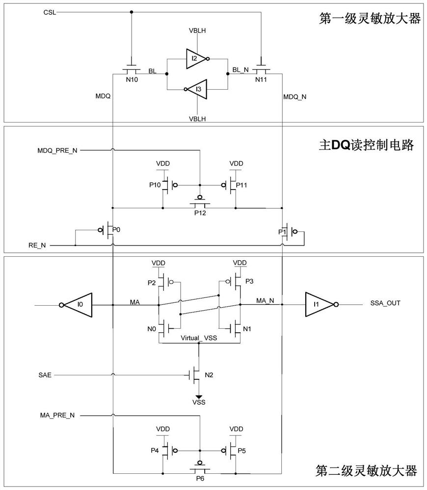
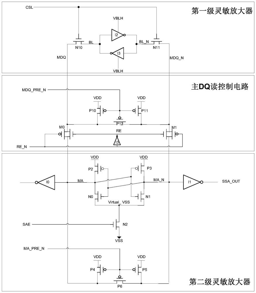
[0061] see figure 2 as shown, figure 2 A write-back circuit for improving the read stability of the sense amplifier of the present invention includes a first-stage sense amplifier, and the NMOS transistor N10 and the NMOS transistor N11 are connected to the first-stage sense amplifier and the main DQ read control circuit; the precharge PMOS transistor P10 and the PMOS The transistor P11 and the balance PMOS transistor P12 form the pre-charging circuit of the main DQ, and the transmission tube M0 and the transmission tube M1 are connected to the main DQ read control circuit and the second-stage sense amplifier.

[0062] The power supply of the first-stage sense amplifier is connected to VBLH, the sources of the NMOS transistor N10 and the NMOS transistor N11 are respectively connected to the bit line BL and the bit line inversion signal BL_N, and the gates of the NMOS transistor N10 and the NMOS transistor N11 are connected to the column selection line CSL signal, The drains...

Embodiment 2

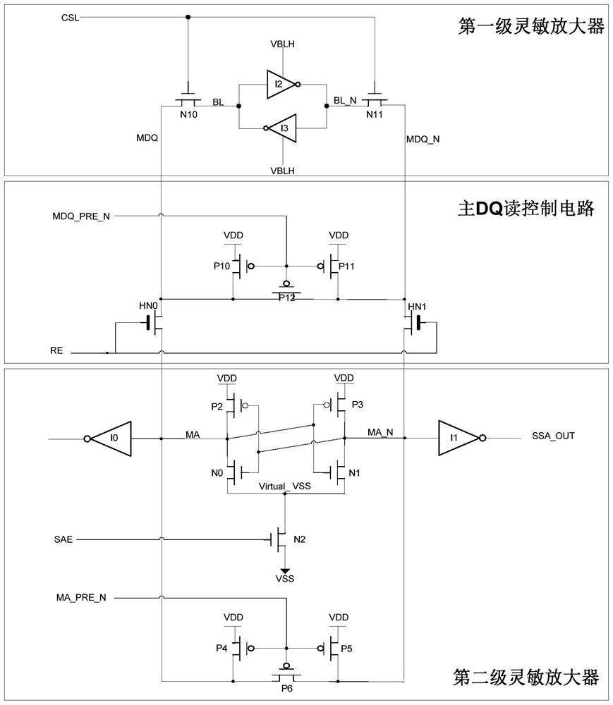
[0070] image 3 Shown is the schematic of the second write-back circuit to improve the read stability of the sense amplifier. Including the first-stage sense amplifier, the NMOS transistor N10 and NMOS transistor N11 are connected to the first-stage sense amplifier and the main DQ read control circuit; the pre-charge PMOS transistor P10, PMOS transistor P11 and equalization PMOS transistor P12 form the pre-charge circuit of the main DQ, thick The gate NMOS transistor HN0 and the transistor HN1 are connected to the main DQ and the second-stage sense amplifier.

[0071] The power supply of the first-stage sense amplifier is connected to VBLH, the sources of NMOS transistor N10 and NMOS transistor N11 are connected to the bit line BL and the bit line inverse signal BL_N, the gates of N10 and N11 are connected to the column selection line CSL signal, and the drains of N10 and N11 The poles are respectively connected to the amplification lines MDQ / MDQ_N.

[0072] The gates of the...


PUM


Abstract

The invention discloses a write-back circuit and a method for improving the reading stability of a sensitive amplifier. The write-back circuit includes: a first-stage sensitive amplifier, which first amplifies data and transmits the amplified data to an amplifying line; The secondary sense amplifier is used for secondary amplification of the amplified data; the main DQ read control circuit is connected to the first level sense amplifier and the second level sense amplifier and kept on; it is used to transmit the amplified data to the second level Sensitive amplifier; and write the secondary amplified data back to the amplifying line, so as to write back the first-stage sense amplifier, and recover the voltage peak coupled on the first-stage sense amplifier bit line BL or BL_N. The write-back circuit for improving the read stability of the sense amplifier of the present invention writes back the signal MA / MA_N amplified by the second-stage sense amplifier to the first-stage sense amplifier. The read stability of the first-stage sense amplifier is improved, and the reliability of the read operation is improved.

Description

technical field [0001] The invention relates to the field of memory design, in particular to a write-back circuit and method for improving the read stability of a sense amplifier. Background technique [0002] Sensitive amplifiers are widely used in memory read operations, mainly for amplifying small signals on bit lines to digital signals. In the memory read operation stage, the first-stage sense amplifier amplifies the small signal read from the array. When the small signal is amplified to a recognizable digital signal, the main DQ (DQ, that is, Data I / O is the input and output line or connection of data Interface) The read control circuit transmits the amplified digital signal to the second-stage sense amplifier, and the signal is amplified twice by the second-stage sense amplifier. [0003] Such as figure 1 Shown is the schematic diagram of the traditional memory read operation data amplification circuit: the operating voltage of the first-stage sense amplifier is the ...

Claims


Application Information

Patent Timeline
Patent Type & Authority Patents(China)
IPC IPC(8): G11C7/06G11C7/08
CPCG11C7/062G11C7/08
Inventor 熊保玉张颖庞理
Owner XI AN UNIIC SEMICON CO LTD
Why Eureka
Try Eureka