


Quick Research
Generate reliable direction feasibility study reports for your R&D in just a few steps.

Technical Q&A
Discover and master advanced knowledge NOW. Basics, ideas, possibilities, all at once.

Find Solutions
As an expert in R&D theories, this can generate solutions to your technical problems instantly.

Evaluate Feasibility
Analyze your overall solution with one click, know your potential R&D risks in advance.

Monitor Landscape
Get weekly tech updates, stay abreast of the latest tech innovations and key insights.
Printed wiring board
A technology for printed wiring substrates and wiring substrates, which is applied in the directions of printed circuits, printed circuits, and printed circuit manufacturing, and can solve the problems of easy suction of flux, narrowing of gaps, and capillary phenomenon.
- Summary
- Abstract
- Description
- Claims
- Application Information
AI Technical Summary
Problems solved by technology
Method used
Image

Examples
no. 1 approach
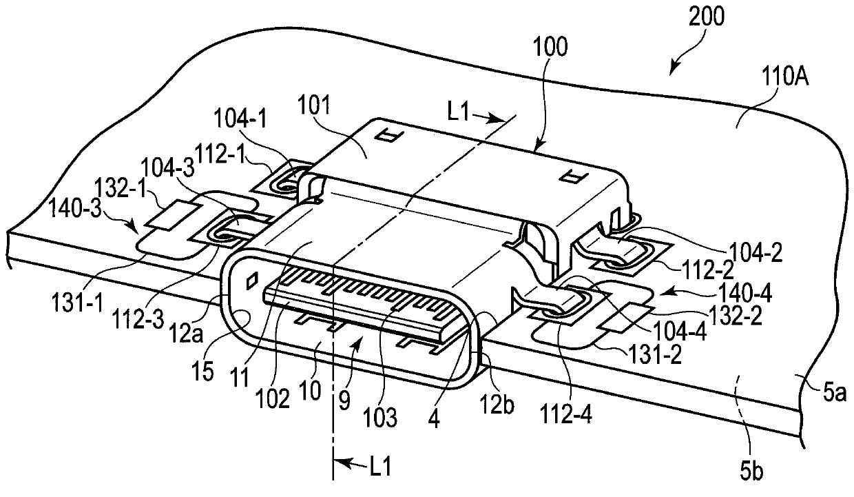
[0034] figure 1 It is a perspective view of a printed wiring board 1 used in electronic equipment such as a mobile phone or a digital camera, for example.
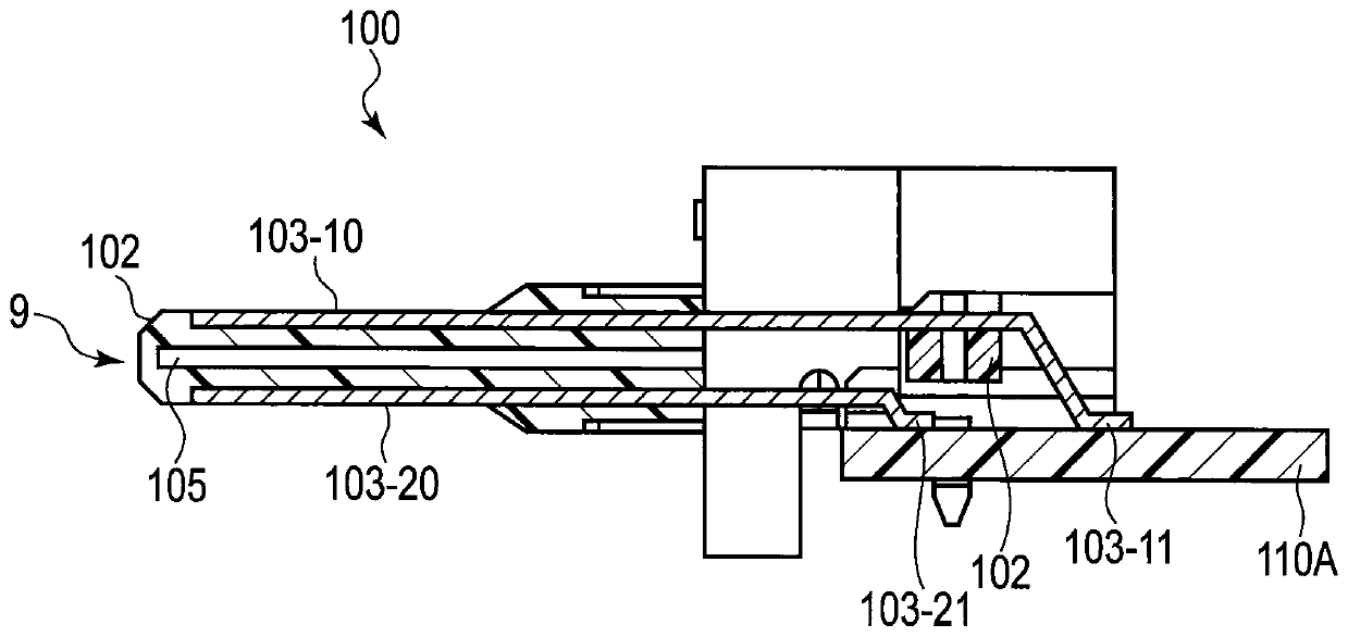
[0035] figure 2 yes figure 1 The L1-L1 sectional view of , but the section of the housing 101 is omitted.
[0036] Such as figure 1 and figure 2 As shown, the printed wiring board 200 of this embodiment includes a wiring board 110A and a USB connector 100 mounted on the wiring board 110A as main elements. The USB connector 100 is an example of a surface mount type connector component.
[0037] According to the present embodiment, wiring board 110A has cutting portion 4 . The cutting portion 4 is cut out to form an opening on one side of the outer peripheral edge of the wiring board 110A. The cutout 4 defines a rectangular space into which the USB connector 100 enters.
[0038] Furthermore, wiring board 110A has flat surface 5 a and rear surface 5 b that are continuous with cut portion 4 . Four reinforcement pads...
no. 2 approach
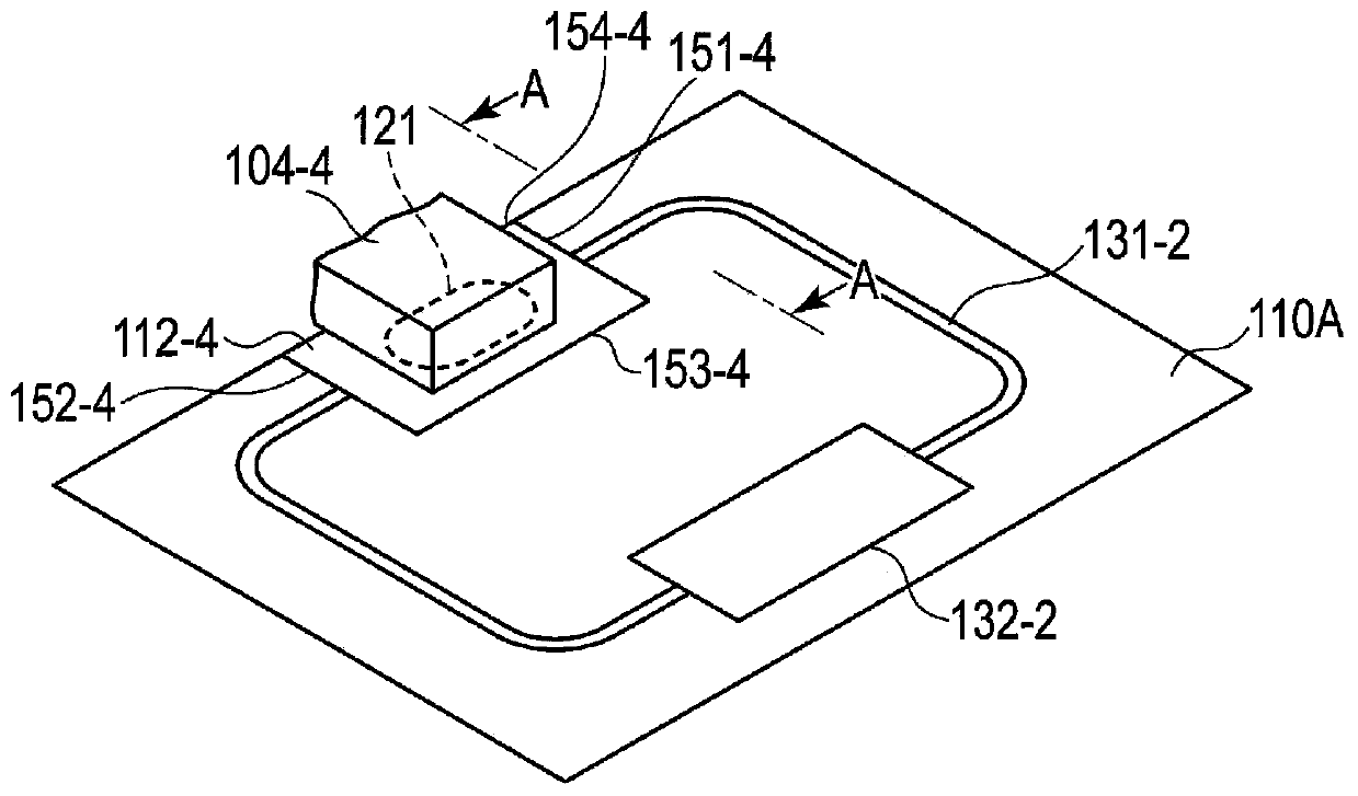
[0075] Figure 7 A schematic diagram showing a state before reflow of the guide groove used in the second embodiment is shown in .
[0076] As shown in the figure, two guide grooves 135 - 2 and 138 - 2 are connected to the reinforcing land 112 - 4 of the wiring board used in the second embodiment. The guide groove 135-2 has a first guide groove 133-2 connected to the side 151-4 of the reinforcement pad 112-4 and extending in a direction from the side 151-4 toward the rear end of the housing 101, and The second guide groove 134 - 2 extends away from the housing 101 in the width direction of the housing 101 continuously from the first guide groove 133 - 2 . In addition, the guide groove 138-2 is the same as the guide groove 135-2, and is connected to the side 152-4 of the reinforcing pad 112-4 that is opposite to the side 151-4, and is connected to the housing 101 from the side 152-4. The first guide groove 136-2 extending in the direction of the front end of the housing 101, ...
no. 3 approach
[0088] Figure 11 A schematic diagram showing a state before reflow of the guide groove used in the third embodiment is shown in .
[0089] As shown in the figure, a wiring board 110C used in the third embodiment is formed by placing a receiving film 140 made of a resin film such as polyimide having a rectangular shape of, for example, a size of 10 mm×10 mm and a thickness of 0.3 mm through an adhesive. Paste on the first guide groove 136-2 connected to the guide groove 138-2 of the reinforcement pad 112-4 to the second guide groove 137-2 to increase the area where capillary phenomenon occurs, and has the same Figure 7 Same composition.
[0090] As a material of a receiving film, heat-resistant resin films, such as PI, PTFE, polyester, are mentioned, for example. In addition to the resin film, porous materials such as ceramics, carbon materials, and porous silica can be used.
[0091] Except for using the wiring board 110C provided with such a guide groove and a receiving ...
PUM
 Abstract
Description
Claims
Application Information
 - R&D Engineer
- R&D Manager
- IP Professional
- Industry Leading Data Capabilities
- Powerful AI technology
- Patent DNA Extraction
Browse by: Latest US Patents, China's latest patents, Technical Efficacy Thesaurus, Application Domain, Technology Topic, Popular Technical Reports.
© 2024 PatSnap. All rights reserved.Legal|Privacy policy|Modern Slavery Act Transparency Statement|Sitemap|About US| Contact US: help@patsnap.com