Liquid crystal panel and display device

A liquid crystal panel and substrate technology, which is applied in the direction of instruments, nonlinear optics, optics, etc., can solve problems affecting the display quality of liquid crystal panels, slow liquid crystal rebound speed, and prone to vacuum bubbles, etc., to improve display quality and volume ratio Uniform, avoid the effect of vacuum bubbles

Active Publication Date: 2021-01-15
TCL CHINA STAR OPTOELECTRONICS TECH CO LTD
View PDF4 Cites 0 Cited by
  • Summary
  • Abstract
  • Description
  • Claims
  • Application Information

AI Technical Summary

Problems solved by technology

Because the flat layer in the conventional first substrate is polytetrafluoroethylene, the material is relatively soft, and the spacer is arranged on the surface of the flat layer. When the liquid crystal panel is pressed, the spacer compresses the flat layer downward, and the flat layer is compressed. The amount of deformation is large, the elastic recovery is also fast, and the rebound speed of the liquid crystal is slow, resulting in a gap in the liquid crystal box, the liquid crystal falls off from the plastic frame, and vacuum bubbles are prone to appear
[0004] To sum up, in the prior art liquid crystal panel, the material of the flat layer on the surface of the first substrate is relatively soft. When the liquid crystal panel is under pressure, the spacers are easily elastically compressed, and the liquid crystal has no time to rebound, resulting in gaps in the liquid crystal layer, and the liquid crystal falls off to form vacuum bubbles. , thus affecting the technical problems of the display quality of the LCD panel, which needs to be improved

Method used


Image

  • Liquid crystal panel and display device
  • Liquid crystal panel and display device
  • Liquid crystal panel and display device

Examples


Embodiment Construction

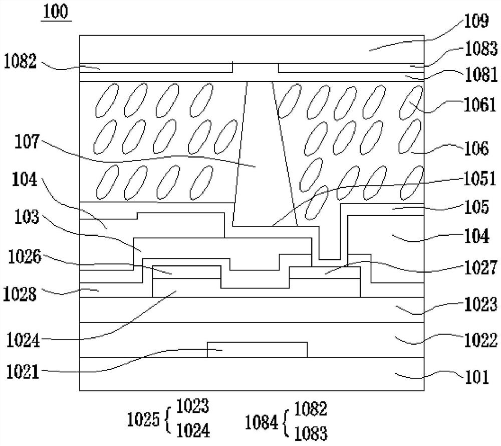
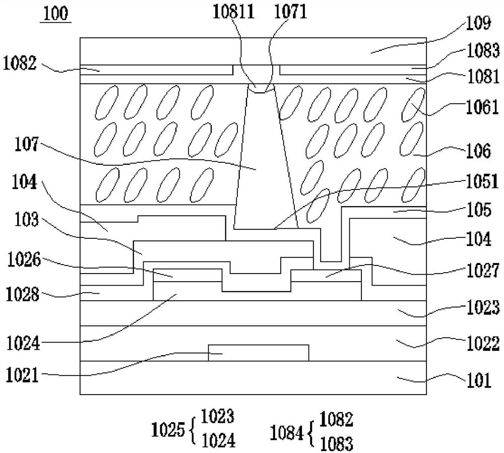
[0024]The description of the following embodiments refers to the attached drawings to illustrate specific embodiments in which the present invention can be implemented. The directional terms mentioned in the present invention, such as [Up], [Down], [Front], [Back], [Left], [Right], [Inner], [Outer], [Side], etc., are for reference only The direction of the additional schema. Therefore, the directional terms used are used to describe and understand the present invention, rather than to limit the present invention. In the figure, the units with similar structures are indicated by the same reference numerals, and the dotted lines in the figure indicate the ones that do not exist in the structure, and merely illustrate the shape and position of the structure.

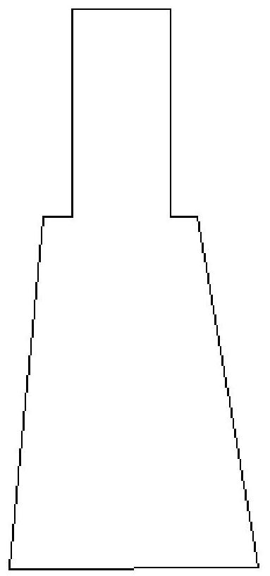
[0025]The present invention aims to solve the problem that the flat layer of the first substrate in the prior art liquid crystal panel is relatively soft. When the liquid crystal panel is pressed, the spacer is easy to be elasticall...


PUM

PropertyMeasurementUnit
thicknessaaaaaaaaaa

Abstract

The present invention provides a liquid crystal panel and a display device. One end of the spacer in the present invention is located on the color resist layer in the first substrate, and the other end is embedded on the common electrode in the second substrate. When the liquid crystal panel is pressed, the color resist The layer material is hard and not easy to compress, which ensures that the deformation recovery speed of the spacer is close to the rebound speed of the liquid crystal. The liquid crystal and the spacer in the liquid crystal layer fill the space in the liquid crystal cell, and the liquid crystal will not peel off from the plastic frame. The formation of vacuum bubbles is avoided, thereby improving the display quality of the liquid crystal panel.

Description

Technical field[0001]The present invention relates to the technical field of liquid crystal display, in particular to a liquid crystal panel and a display device.Background technique[0002]The liquid crystal panel includes a first substrate and a second substrate arranged in a cell, and a liquid crystal layer located between the first substrate and the second substrate. The spacer is located on the surface of the first substrate and extends to the second substrate for The role of supporting box thickness.[0003]In the liquid crystal cell, the volume ratio of the liquid crystal and the spacer is uniform, filling the space in the liquid crystal cell, the liquid crystal will not peel off from the plastic frame, and the liquid crystal panel displays normally. Since the flat layer in the conventional first substrate is made of PTFE, the material is relatively soft, and the spacers are arranged on the surface of the flat layer. When the liquid crystal panel is pressed, the spacers compress ...

Claims


Application Information

Patent Timeline
Patent Type & Authority Patents(China)
IPC IPC(8): G02F1/1339G02F1/1362G02F1/1333G02F1/1343
CPCG02F1/1333G02F1/13394G02F1/1343G02F1/1362G02F1/133357G02F1/13398G02F1/136222
Inventor 余佳佳
Owner TCL CHINA STAR OPTOELECTRONICS TECH CO LTD
Why Eureka
Try Eureka