
Level conversion circuit and level conversion method

A technology for converting circuits and levels, applied in the direction of logic circuit connection/interface layout, logic circuit coupling/interface using field effect transistors, etc., can solve problems such as conversion, achieve simple overall structure, reduce response time, and power consumption low effect

Inactive Publication Date: 2020-01-24
HUAZHONG UNIV OF SCI & TECH
View PDF8 Cites 6 Cited by
  • Summary
  • Abstract
  • Description
  • Claims
  • Application Information

AI Technical Summary

Problems solved by technology

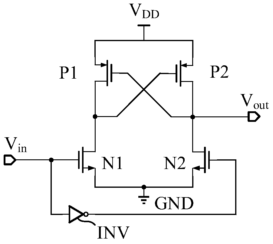
[0004] In view of the defects of the prior art, the purpose of the present invention is to solve the technical problem that the low-level signal whose voltage domain is lower than the threshold voltage of the NMOS transistor cannot be converted into a high-level signal through the existing level conversion circuit

Method used


Image

  • Level conversion circuit and level conversion method
  • Level conversion circuit and level conversion method
  • Level conversion circuit and level conversion method

Examples


Embodiment Construction

[0038] In order to make the object, technical solution and advantages of the present invention clearer, the present invention will be further described in detail below in conjunction with the accompanying drawings and embodiments. It should be understood that the specific embodiments described here are only used to explain the present invention, not to limit the present invention. In addition, the technical features involved in the various embodiments of the present invention described below can be combined with each other as long as they do not constitute a conflict with each other.

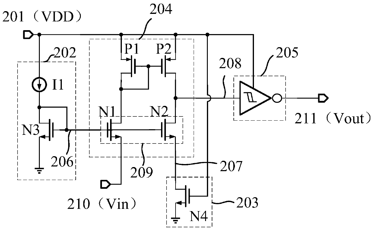
[0039] The invention discloses a level conversion circuit from ultra-low voltage to high voltage. The circuit includes a bias voltage generating unit, a threshold voltage generating unit, a differential common-gate amplifier, and a hysteretic inverter. The input terminal of the bias voltage generating unit is connected to the power supply voltage, and the output terminal is connected to the bias...


PUM


Abstract

The invention discloses a level conversion circuit and a level conversion method. The level conversion circuit comprises a current mirror, a first NMOS transistor and a second NMOS transistor, gates of the first NMOS transistor and the second NMOS transistor are connected to the same bias voltage. A drain electrode of the first NMOS tube is connected with one side of the current mirror, and the drain electrode of the second NMOS tube is connected with the other side of the current mirror. The source electrode of the first NMOS transistor is connected with an input voltage, and the source electrode of the second NMOS transistor is connected with a threshold voltage; the first NMOS transistor and the second NMOS transistor convert the input voltage and the threshold voltage into corresponding currents respectively and input the currents to the two sides of the current mirror; the current mirror compares two currents input from the first NMOS tube and the second NMOS tube, converts the two currents into corresponding voltages and outputs the voltages from the other side of the current mirror; the first input end of the hysteresis inverter is connected with voltage output by the current mirror, and the second input end is connected with power supply voltage; and when the input voltage is greater than the threshold voltage, the voltage output by the current mirror is zero, and the output voltage of the hysteresis inverter is the power supply voltage. According to the invention, the requirement on an input signal is reduced, and level conversion is realized.

Description

technical field [0001] The present invention relates to the technical field of analog integrated circuits, and more specifically, to a level conversion circuit and a level conversion method. Background technique [0002] As integrated circuits become more integrated, more and more circuit modules with different functions will be integrated into one chip. However, because different circuit modules in the chip have different power requirements, such as low power consumption circuits generally require low power supply voltages, high-speed communication chips require higher power supply voltages to increase their voltage conversion rates, and different chips also require There will be different voltage domains. Therefore, a level conversion circuit is required to enable signals to be transmitted between different voltage domains. It should be noted that when the signal is transferred from the low-voltage domain to the high-voltage domain, if the level conversion circuit cannot...

Claims


Application Information

Patent Timeline
Patent Type & Authority Applications(China)
IPC IPC(8): H03K19/0185
CPCH03K19/0185
Inventor 邹志革徐文韬邹雪城皮庆广童乔凌
Owner HUAZHONG UNIV OF SCI & TECH
Learn More