Electromagnetic shielding film, circuit board and preparation method of electromagnetic shielding film

An electromagnetic shielding film and circuit board technology, applied in the electronic field, can solve problems such as grounding failure, inability to interfere with charge derivation, and peeling off

Pending Publication Date: 2020-01-14
GUANGZHOU FANGBANG ELECTRONICS
View PDF4 Cites 0 Cited by
  • Summary
  • Abstract
  • Description
  • Claims
  • Application Information

AI Technical Summary

Problems solved by technology

However, in the process of implementing the present invention, the inventors have found that there are at least the following problems in the prior art: there are volatiles in the conductive adhesive layer under high temperature conditions, but the shielding layer is relatively dense, and the volatiles are difficult to discharge, which leads to electromagnetic shielding films. Bubble delamination causes peeling between the electromagnetic shielding film and the ground layer of the circuit board, which in turn leads to grounding failure and the inability to export interference charges

Method used


Image

  • Electromagnetic shielding film, circuit board and preparation method of electromagnetic shielding film
  • Electromagnetic shielding film, circuit board and preparation method of electromagnetic shielding film
  • Electromagnetic shielding film, circuit board and preparation method of electromagnetic shielding film

Examples


Embodiment Construction

[0040] The following will clearly and completely describe the technical solutions in the embodiments of the present invention with reference to the accompanying drawings in the embodiments of the present invention. Obviously, the described embodiments are only some of the embodiments of the present invention, not all of them. Based on the embodiments of the present invention, all other embodiments obtained by persons of ordinary skill in the art without creative efforts fall within the protection scope of the present invention.

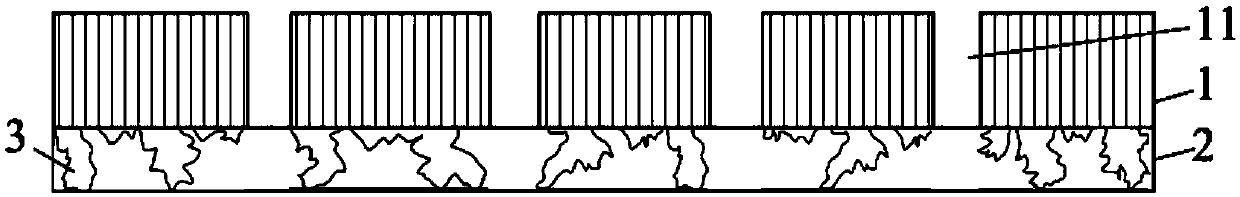
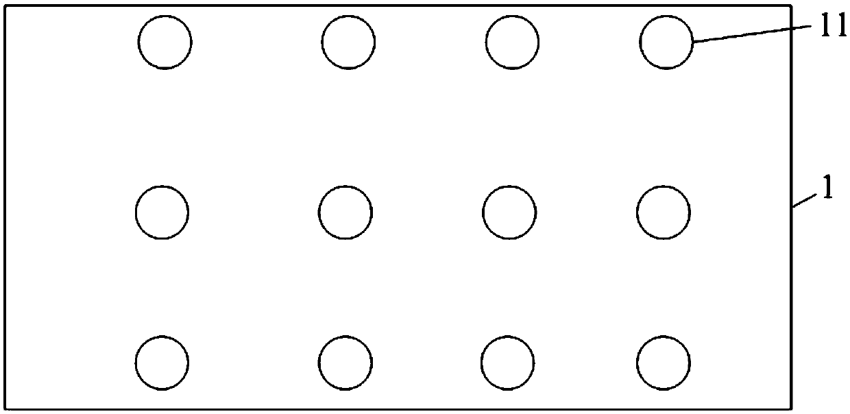
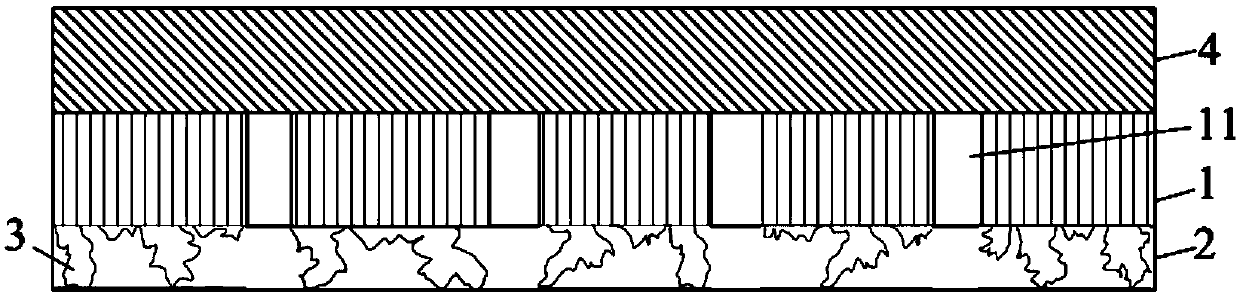
[0041] to combine Figure 1 to Figure 4 As shown, an electromagnetic shielding film according to a preferred embodiment of the present invention includes a shielding layer 1 and an adhesive film layer 2, and the adhesive film layer 2 is arranged on the shielding layer 1; The through holes 11 on the upper and lower surfaces, the side of the shielding layer 1 close to the adhesive film layer 2 is a flat surface, and the side of the shielding layer 1 clo...


PUM

PropertyMeasurementUnit
heightaaaaaaaaaa
thicknessaaaaaaaaaa
thicknessaaaaaaaaaa

Abstract

The invention relates to the technical field of electronics, and discloses an electromagnetic shielding film, a circuit board, and a preparation method of the electromagnetic shielding film. The electromagnetic shielding film comprises a shielding layer and an adhesive film layer. The adhesive film layer is arranged on the shielding layer. The surface, which is near the adhesive film layer, of theshielding layer is a flat surface. The shielding layer is provided with through holes penetrating the upper and lower surfaces thereof, which is beneficial for volatiles in the adhesive film layer tobe exhausted through the through holes in the shielding layer at high temperature. Volatiles in the adhesive film layer can be easily discharged at high temperature. The electromagnetic shielding film is prevented from being peeled off from the ground layer of the circuit board due to bubbling and delamination of the electromagnetic shielding film. The electromagnetic shielding film is grounded,and interference charges are led out. In addition, the side, which is close to the adhesive film layer, of the shielding layer is provided with convex conductor particles. The conductor particles canpierce the adhesive film layer and is connected with the ground layer of the circuit board when the electromagnetic shielding film is laminated with the circuit board. The connection of the shieldinglayer and the ground layer of the circuit board is ensured.

Description

technical field [0001] The invention relates to the field of electronic technology, in particular to an electromagnetic shielding film, a circuit board and a preparation method of the electromagnetic shielding film. Background technique [0002] With the rapid development of the electronics industry, electronic products are further developed toward miniaturization, light weight, and high-density assembly, which greatly promotes the development of flexible circuit boards, thereby realizing the integration of component devices and wire connections. Flexible circuit boards can be widely used in industries such as mobile phones, liquid crystal displays, communications and aerospace. [0003] Driven by the international market, functional flexible circuit boards dominate the flexible circuit board market, and an important indicator for evaluating the performance of functional flexible circuit boards is Electromagnetic Interference Shielding (EMI Shielding). With the integration ...

Claims


Application Information

Patent Timeline
Patent Type & Authority Applications(China)
IPC IPC(8): H05K9/00H05K1/02C09J7/20C09J9/02B32B33/00B32B7/06
CPCH05K9/0084H05K1/0218C09J7/20C09J9/02B32B33/00B32B7/06H05K2201/0715B32B2307/212C09J2301/18C09J2301/122
Inventor 苏陟
Owner GUANGZHOU FANGBANG ELECTRONICS
Why Eureka
Try Eureka