
Chip packaging box and chip packaging method

A packaging box and chip technology, applied in the field of packaging, can solve problems such as vacuum packaging failure, frequent shaking or friction of chips, chip structure damage, etc., achieve good strength and cushioning performance, save material costs, and prevent contamination.

Inactive Publication Date: 2020-01-14
SUZHOU TF AMD SEMICON CO LTD
View PDF5 Cites 3 Cited by
  • Summary
  • Abstract
  • Description
  • Claims
  • Application Information

AI Technical Summary

Problems solved by technology

[0003] 1. At present, in the process of chip manufacturing, storage and transportation, industry-standard injection trays are generally used, and the material is hard engineering plastic. When the weight of the chip is large, the vibration and impact during the transportation process will cause the chip to shake and rub in the tray. , it is easy to cause damage or failure of the chip structure, the chip frequently shakes or rubs in the tray, and it is easy to cause the tray material to fall off and contaminate the chip
[0004] 2. Aluminum foil bags and similar barrier bags made of polymer materials are limited in structure and process. Although they are multi-layered, their thickness is very thin, and they are easily damaged or damaged during transportation, resulting in air leakage, which makes the vacuum packaging invalid.
[0005] 3. The packaging operation is cumbersome, and the pallets need to be packed, bagged, vacuumed and sealed, wrapped in cushioning materials and boxed many times, and the efficiency is low

Method used


Image

  • Chip packaging box and chip packaging method
  • Chip packaging box and chip packaging method
  • Chip packaging box and chip packaging method

Examples


Embodiment Construction

[0044] The application will be further described in detail below in conjunction with the accompanying drawings and embodiments. It should be understood that the specific embodiments described here are only used to explain related inventions, rather than to limit the invention. It should also be noted that, for ease of description, only parts related to the invention are shown in the drawings.

[0045] It should be noted that, in the case of no conflict, the embodiments in the present application and the features in the embodiments can be combined with each other. The present application will be described in detail below with reference to the accompanying drawings and embodiments.

[0046] As mentioned in the background technology, the current main form of chip packaging in the packaging and testing industry is: the chip is loaded in an injection tray, and then put in an aluminum foil bag with a desiccant or a similar high-barrier vacuum packaging bag, Vacuum the inside of th...


PUM


Abstract

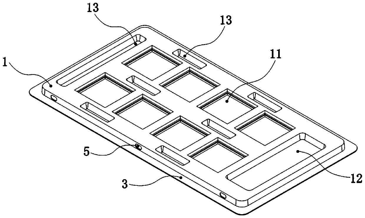
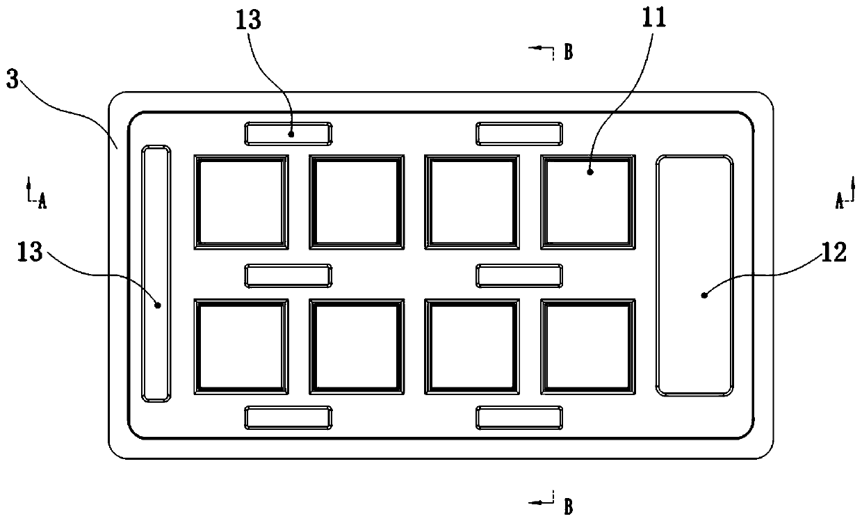
The invention discloses a chip packaging box and a chip packaging method. The chip packaging box comprises a first cover body and a second cover body. The first cover body and the second cover body are of stereoscopic structures formed by die hot pressing or vacuum plastic uptake, and first grooves for containing chips and second grooves for containing auxiliary materials are formed in the first cover body. A first scrap is arranged on the outer side of the first cover body, a second scrap is arranged on the outer side of the second cover body, the second cover body is buckled on the first cover body, the first scrap and the second scrap are subjected to heat sealing, the chips can be packaged, the operation is easy, and the efficiency is high. Firstly, the first cover body and the secondcover body have good strength and buffer performance, protection of the chips is good, the chips are not easily broken, scraps do not easily fall, and the chips can be prevented from being contaminated. The packaging box has a good barrier property after heat sealing, the packaging box can be used for transportation and directly used for chip drying and packaging, and the material cost of a dryingand packaging bag is reduced.

Description

technical field [0001] The present application generally relates to the technical field of packaging, and in particular relates to a chip packaging box and a chip packaging method. Background technique [0002] Chips, especially high-end chips, are of high value but are easily damaged or invalidated, so there are extremely high requirements for their packaging protection. Chips are moisture-sensitive components, and some components are easily oxidized, so they need to be stored in a low-humidity environment or even a low-oxygen environment. At present, the main form of chip packaging in the packaging and testing industry is: the chip is loaded in an injection tray, and then put into an aluminum foil bag with a desiccant or a similar high-barrier vacuum packaging bag, and then the bag is vacuumed and then cleaned. The mouth of the bag is heat-sealed, then wrapped with cushioning material and packed into a carton. But the above method has the following problems: [0003] 1....

Claims


Application Information

Patent Timeline
Patent Type & Authority Applications(China)
IPC IPC(8): B65D85/86B65D1/36B65D1/40
CPCB65D1/36B65D1/40B65D85/70B65D2585/86
Inventor 边兵兵焦洁王港善
Owner SUZHOU TF AMD SEMICON CO LTD
Learn More