Flexible device transition device and preparation method and flexible device patch method

A technology of flexible devices and devices, applied in the direction of piezoelectric devices/electrostrictive devices, microstructure devices composed of deformable elements, electric solid devices, etc., can solve the unfavorable development of flexible electronic products and the difficulty of replacing flexible devices , complex equipment and other issues

Active Publication Date: 2019-12-10
INST OF FLEXIBLE ELECTRONICS TECH OF THU ZHEJIANG
View PDF5 Cites 1 Cited by
  • Summary
  • Abstract
  • Description
  • Claims
  • Application Information

AI Technical Summary

Problems solved by technology

This kind of manufacturing technology is not compatible with the existing integrated manufacturing technology and equipment of electronic products. The equipment required for printing or printing technology is complicated and the cost is high, which is not conducive to the development of the flexible electronic product industry.
[0004] In addition, this manufacturing method is not conducive to the screening of devices. If there is a problem with a flexible device based on a polymer substrate, it will affect the function of the entire flexible electronic product. The replacement has a serious impact on the yield of the product
[0005] Finally, in the manufacturing process of flexible electronic products, the placement of IC chips and flexible devices based on polymer substrates requires two completely different sets of equipment, which increases production costs

Method used


Image

  • Flexible device transition device and preparation method and flexible device patch method
  • Flexible device transition device and preparation method and flexible device patch method
  • Flexible device transition device and preparation method and flexible device patch method

Examples


Embodiment Construction

[0077] In order to further explain the technical means and functions adopted by the present invention to achieve the intended invention purpose, the detailed description is as follows in conjunction with the accompanying drawings and preferred embodiments.

[0078] The invention provides a transition device for a flexible device, a method for preparing the transition device and a method for patching a flexible device based on the transition device of the flexible device. The transition device for the flexible device can be easily attached to a polymer substrate SMT processing of flexible devices is convenient for storage and transportation, and it is convenient for mass production of devices with the same specification parameters. The transition device of the flexible device can be directly used in the manufacturing process of flexible electronic products, which is conducive to the development of the flexible electronic product industry. .

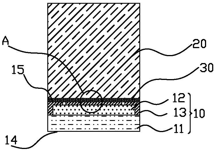
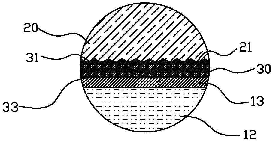
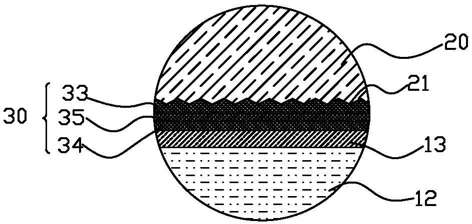
[0079] Such as figure 1 As shown, ...


PUM

PropertyMeasurementUnit
Thicknessaaaaaaaaaa
Thicknessaaaaaaaaaa

Abstract

The invention provides a flexible device transition device and preparation method and a flexible device patch method. The transition device comprises a flexible device based on a polymer substrate anda transition substrate. The flexible device based on the polymer substrate comprises a substrate layer, a device function layer and a packaging layer. The device function layer is arranged on the substrate layer. The packaging layer packages the device function layer. A first surface prepared to be patched with the substrate and a second surface corresponding to the first surface are formed on the flexible device based on the polymer substrate. The transition substrate is bonded to the second surface of the flexible device based on the polymer substrate through an adhesive layer. The flexibledevice transition device can easily perform patch processing on the flexible device based on the polymer substrate, facilitate mass preparation of devices with the same specifications and parametersso that the flexible device transition device is enabled to be directly used in the manufacturing process of flexible electronic products, and the development of the flexible electronic product industry can be facilitated.

Description

technical field [0001] The invention relates to the field of chip packaging, in particular to a transition device for flexible devices, a method for preparing the transition device, and a method for bonding flexible devices based on the transition device for flexible devices. Background technique [0002] In recent years, with the continuous development and progress of flexible electronics technology and the increasingly widespread application of smart wearable products, flexible electronic devices are very popular in the market due to their unique advantages of flexibility, ductility, light weight, and thin thickness. Broad application prospects. [0003] Functional components are the key to the composition of flexible electronic products. Functional components include IC chips based on semiconductor materials such as Si, SiC, and GaAs, and polymer-based polymer substrates such as resistors, capacitors, sensors, and biological MEMS. substrate for flexible devices. Flexibl...

Claims


Application Information

Patent Timeline
IPC IPC(8): H01L27/32B81B3/00B81C1/00
CPCB81B3/00B81C1/00134H10K59/88H10K59/00
Inventor 龚云平
Owner INST OF FLEXIBLE ELECTRONICS TECH OF THU ZHEJIANG
Why Eureka
Try Eureka