Polycrystalline silicon solar cell with high photoelectric conversion efficiency and method for preparing same
A technology for photoelectric conversion efficiency and solar cells, which is applied in photovoltaic power generation, circuits, electrical components, etc., and can solve the problems of poor uniformity of silicon wafer texture and unfavorable photoelectric conversion efficiency of polycrystalline silicon solar cells.
- Summary
- Abstract
- Description
- Claims
- Application Information
AI Technical Summary
Problems solved by technology
Method used
Image
Examples
Embodiment 1
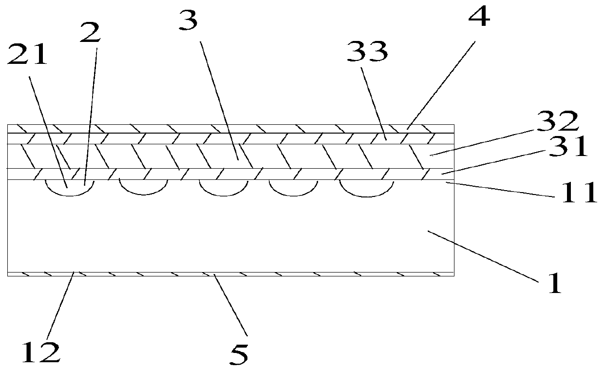
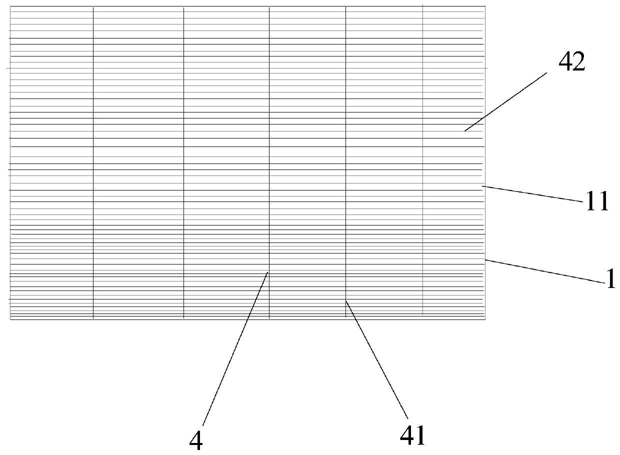
[0066] A polycrystalline silicon solar cell with high photoelectric conversion efficiency, the polycrystalline silicon solar cell includes a polycrystalline silicon chip 1, the front side 11 of the polycrystalline silicon chip 1 is a textured surface 2 formed by etching and textured, and the depth of the groove 21 of the textured surface 2 is 3 μm, The length of the groove 22 of the suede 2 is 8 μm, the width of the groove 22 of the suede 2 is 1 μm, and three layers of anti-reflection films 3 are deposited on the upper surface of the suede 2, and the three layers of anti-reflection films 3 are all silicon nitride films. The layer anti-reflection film 3 includes a first layer of film 31, a second layer of film 32 and a third layer of film 33. The first layer of film 31 covers the front side 11 of the polysilicon wafer 1 and has a first refractive index and a first thickness. A layer of film 32 covers the upper surface of the first layer of film 31 and has a second refractive ind...
Embodiment 2
[0086] A polycrystalline silicon solar cell with high photoelectric conversion efficiency, the polycrystalline silicon solar cell includes a polycrystalline silicon chip 1, the front side 11 of the polycrystalline silicon chip 1 is a textured surface 2 formed by etching and textured, and the depth of the groove 21 of the textured surface 2 is 3.2 μm , the length of the groove 21 of the suede 2 is 8.5 μm, the width of the groove 21 of the suede 2 is 1.5 μm, and three layers of anti-reflection films 3 are deposited on the upper surface of the suede 2, and the three layers of anti-reflection films 3 are silicon nitride The three-layer anti-reflection film 3 includes a first layer of film 31, a second layer of film 32 and a third layer of film 33. The first layer of film 31 covers the front side 11 of the polysilicon wafer 1 and has a first refractive index and a first thickness. , the second layer of film 32 covers the upper surface of the first layer of film 31 and has a second r...
Embodiment 3
[0106] A polycrystalline silicon solar cell with high photoelectric conversion efficiency, the polycrystalline silicon solar cell includes a polycrystalline silicon chip 1, the front side 11 of the polycrystalline silicon chip 1 is a textured surface 2 formed by etching the textured surface, and the depth of the groove 21 of the textured surface 2 is 3.5 μm , the length of the groove 21 of the textured surface 2 is 10 μm, the width of the groove 21 of the textured surface 2 is 2 μm, and three layers of anti-reflection films 3 are deposited on the upper surface of the textured surface 2, and the three layers of anti-reflection films 3 are all silicon nitride films, The three-layer anti-reflection film 3 includes a first layer of film 31, a second layer of film 32 and a third layer of film 33. The first layer of film 31 covers the front side 11 of the polysilicon wafer 1 and has a first refractive index and a first thickness. The second layer of film 32 covers the upper surface o...
PUM
| Property | Measurement | Unit |
|---|---|---|
| First thickness | aaaaa | aaaaa |
| Second thickness | aaaaa | aaaaa |
| Depth | aaaaa | aaaaa |
Abstract
Description
Claims
Application Information
 - R&D
- Intellectual Property
- Life Sciences
- Materials
- Tech Scout
- Unparalleled Data Quality
- Higher Quality Content
- 60% Fewer Hallucinations
Browse by: Latest US Patents, China's latest patents, Technical Efficacy Thesaurus, Application Domain, Technology Topic, Popular Technical Reports.
© 2025 PatSnap. All rights reserved.Legal|Privacy policy|Modern Slavery Act Transparency Statement|Sitemap|About US| Contact US: help@patsnap.com


