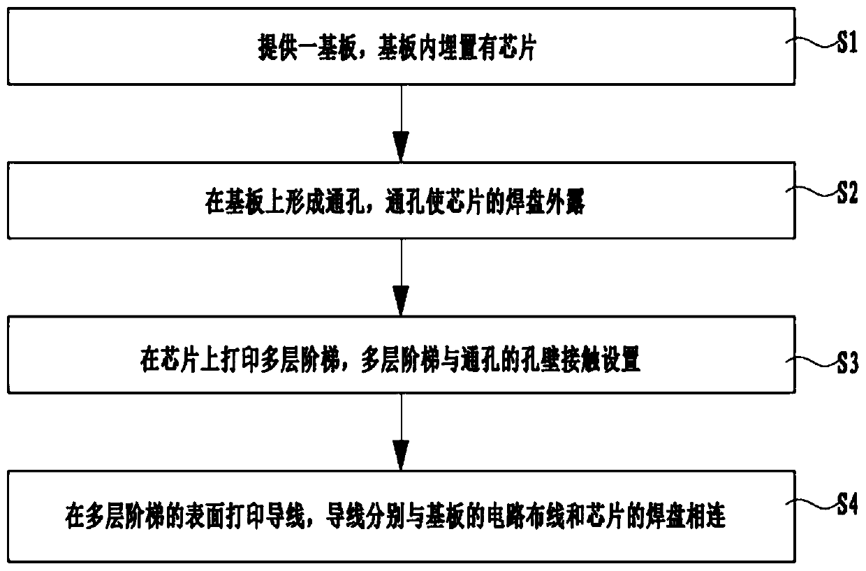
Chip interconnection packaging method and interconnection packaging structure
An encapsulation method and encapsulation structure technology, applied in the directions of electrical components, electrical solid devices, circuits, etc., can solve the problems of breakage, peeling off, metal stripping of through holes, and unstable electrical conductivity of wires 30, so as to improve reliability, The effect of dispersing stress and improving the reliability of electrical connection
- Summary
- Abstract
- Description
- Claims
- Application Information
AI Technical Summary
Problems solved by technology
Method used
Image

Examples
Embodiment 1
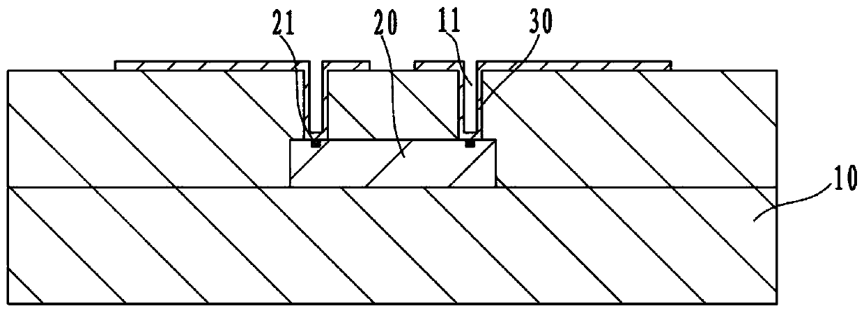
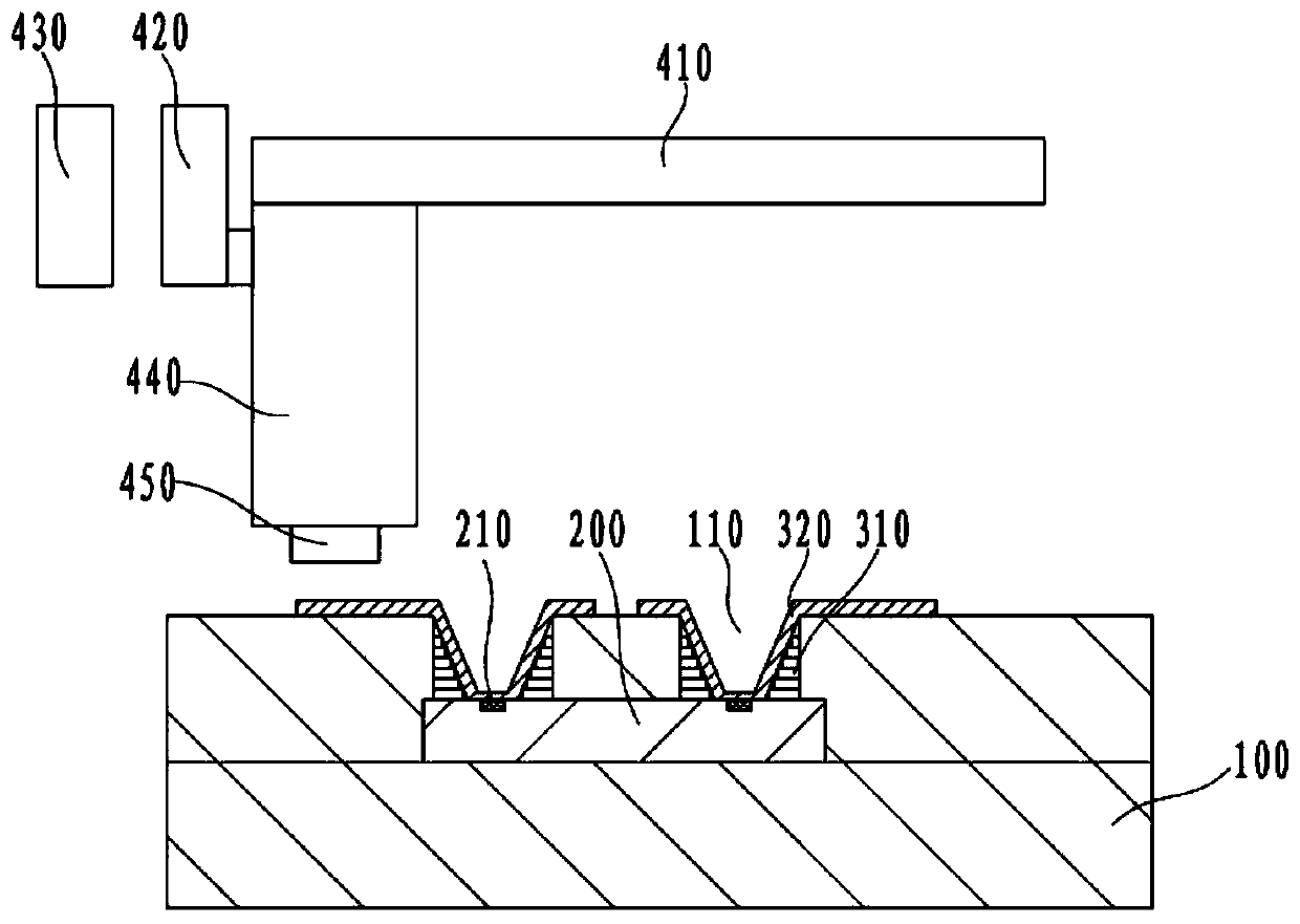
[0053] (1) Laser drilling: laser drilling, the prepared through hole 110 has an inner diameter of 65 μm and a depth of 50 μm;
[0054] (2) Preparation of multi-layer ladder 310: Yiligao URC-TDS has a viscosity of 500 mPas as the material for preparing multi-layer ladder 310, and its viscosity is 500 mPas. One layer of steps, the first step has a width of 20 μm and a height of 20 μm;
[0055](3) Curing molding: curing at 120°C for 60 minutes;
[0056] (4) Preparation of multi-layer ladder 310: Elektro URC-TDS is used as the material for preparing multi-layer ladder 310, and its viscosity is 120 mPas. The second layer of ladder is printed by inkjet printing equipment, and the width of the second layer of ladder is 15 μm. The height is 15 μm;
[0057] (5) Curing molding: curing at 120°C for 60 minutes;
[0058] (6) Preparation of multi-layer ladder 310: Elektro URC-TDS is used as the material for preparing multi-layer ladder 310, and its viscosity is 120 mPas. The third layer ...
Embodiment 2
[0067] (1) Laser drilling: laser drilling, the prepared through hole 110 has an inner diameter of 150 μm and a depth of 100 μm;
[0068] (2) Preparation of multi-layer ladder 310: Elektro URC-TDS is used as the material for preparing multi-layer ladder 310, its viscosity is 120mPas, the printing equipment is SIJ SuperInkjetPrinter printer, and the first layer of ladder is printed by inkjet printing through the printing equipment, the second A step width of 60 μm and a height of 20 μm;
[0069] (3) Curing molding: curing at 120°C for 60 minutes;
[0070] (4) Preparation of multi-layer ladder 310: Elektro URC-TDS is used as the material for preparing multi-layer ladder 310, and its viscosity is 120 mPas. The second layer of ladder is printed by inkjet printing equipment, and the width of the second layer of ladder is 40 μm. The height is 20 μm;
[0071] (5) Curing molding: curing at 120°C for 60 minutes;
[0072] (6) Preparation of multi-layer ladder 310: Elektro URC-TDS is u...
Embodiment 3
[0085] (1) Laser drilling: laser drilling, the prepared through hole 110 has an inner diameter of 200 μm and a depth of 100 μm;
[0086] (2) Preparation of multi-layer ladder 310: CYCLOTENE3000 series BCB solution is used as the material for preparing multi-layer ladder 310, its viscosity is 10000mPas, the printing equipment is SIJ SuperInkjetPrinter printer, the first layer of ladder is printed by inkjet printing through the printing equipment, the first layer The step width is 80 μm and the height is 20 μm;
[0087] (3) Pre-curing molding: curing at 120°C for 5 minutes;
[0088] (4) Preparation of multi-layer ladder 310: CYCLOTENE3000 series BCB solution is used as the material for preparing multi-layer ladder 310, its viscosity is 10000mPas, the second layer of ladder is printed by inkjet printing equipment, the width of the second layer of ladder is 60μm, and the height is 20μm;
[0089] (5) Pre-curing molding: curing at 120°C for 5 minutes;
[0090] (6) Preparation of ...
PUM
| Property | Measurement | Unit |
|---|---|---|
| Thickness | aaaaa | aaaaa |
| Diameter | aaaaa | aaaaa |
| The inside diameter of | aaaaa | aaaaa |
Abstract
Description
Claims
Application Information
 - R&D Engineer
- R&D Manager
- IP Professional
- Industry Leading Data Capabilities
- Powerful AI technology
- Patent DNA Extraction
Browse by: Latest US Patents, China's latest patents, Technical Efficacy Thesaurus, Application Domain, Technology Topic.
© 2024 PatSnap. All rights reserved.Legal|Privacy policy|Modern Slavery Act Transparency Statement|Sitemap