Fingerprint imaging module and forming method thereof, fingerprint imaging module mother board and electronic equipment

An imaging module and fingerprint technology, which is applied in the directions of acquiring/arranging fingerprints/palmprints, printing image collection, character and pattern recognition, etc., can solve the problems affecting the performance, imaging quality and module integration of optical fingerprint imaging modules. Taking into account other issues to achieve the effect of improving the uniformity of incident light, reducing impact and damage, and increasing light intensity

Active Publication Date: 2019-11-15
SHANGHAI OXI TECH
View PDF10 Cites 0 Cited by
  • Summary
  • Abstract
  • Description
  • Claims
  • Application Information

AI Technical Summary

Problems solved by technology

[0004] However, in existing optical fingerprint imaging modules, it is often difficult to balance the imaging quality and module integration, which affects the performance of optical fingerprint imaging modules.

Method used


Image

  • Fingerprint imaging module and forming method thereof, fingerprint imaging module mother board and electronic equipment
  • Fingerprint imaging module and forming method thereof, fingerprint imaging module mother board and electronic equipment
  • Fingerprint imaging module and forming method thereof, fingerprint imaging module mother board and electronic equipment

Examples


Embodiment Construction

[0042] It can be seen from the background art that the fingerprint imaging module in the prior art has the problem that it is often difficult to balance the imaging quality and the integration degree of the module. The reason is analyzed in combination with the structure of the existing fingerprint imaging module.

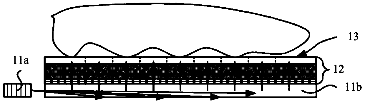
[0043] refer tofigure 1 , shows a schematic cross-sectional structure of a fingerprint imaging module.

[0044] like figure 1 As shown, the fingerprint imaging module is an ultra-thin optical fingerprint imaging module. The fingerprint imaging module realizes fingerprint imaging through the principle of photoelectric conversion, including: a light source, an optical area sensor 12 located on the light source, and a sensing surface 13 located on the optical area sensor 12 .

[0045] When collecting fingerprints, the finger is pressed on the sensing surface 13; the incident light produced by the light source is projected onto the sensing surface 13, and reflection ...


PUM


Abstract

The invention discloses a fingerprint imaging module and a forming method thereof, a fingerprint imaging module mother board and electronic equipment. The fingerprint imaging module comprises a substrate; a light-emitting structure layer, wherein the light-emitting structure layer is located on one surface of the substrate; a pixel array, wherein the pixel array is located on the light-emitting structure layer. Light rays generated by the light-emitting structure layer form sensing light carrying fingerprint information on a sensing surface after transmitting the pixel array, and the pixel array collects the sensing surface to obtain a fingerprint image. The light-emitting structure layer and the pixel array are sequentially stacked on the same surface of the substrate. Therefore, the light source for generating the light and the base layer of the image sensor for collecting the sensing light are realized, the light path for obtaining the fingerprint image light is shortened, and the thickness of the fingerprint imaging module is reduced, so that the aims of improving the integration degree of the device and improving the imaging quality are fulfilled.

Description

technical field [0001] The invention relates to the field of fingerprint imaging, in particular to a fingerprint imaging module and its forming method, a motherboard of the fingerprint imaging module, and electronic equipment. Background technique [0002] The fingerprint identification technology collects the fingerprint image of the human body through the fingerprint imaging module, and then compares it with the existing fingerprint imaging information in the fingerprint identification system to realize identity identification. Due to the convenience of use and the uniqueness of human fingerprints, fingerprint recognition technology has been widely used in various fields, such as: public security bureaus, customs and other security inspection fields, building access control systems, and consumer products such as personal computers and mobile phones, etc. [0003] The imaging methods of the imaging module used in the fingerprint identification technology include optical, ca...

Claims


Application Information

Patent Timeline
Patent Type & Authority Applications(China)
IPC IPC(8): G06K9/00G06K9/20
CPCG06V40/1318G06V10/147
Inventor 辛胜朱虹陆震生管钰晟
Owner SHANGHAI OXI TECH
Why Eureka
Try Eureka