Display screen and display device comprising display screen
A display and encapsulation layer technology, applied in the field of OLED displays, can solve problems such as high cost, cumbersome process, and affecting product yield
- Summary
- Abstract
- Description
- Claims
- Application Information
AI Technical Summary
Problems solved by technology
Method used
Image
Examples
Embodiment 1
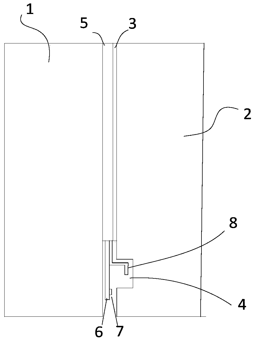
[0047] This embodiment provides a display body, such as figure 1 As shown, it includes a substrate 1 and an anode layer, an organic light-emitting layer, a cathode layer and an encapsulation layer 2 stacked on the surface of the substrate 1 in sequence, and also includes: a groove 4 arranged on the encapsulation layer 2 close to the cathode layer At least one anode conductive coating 7 and at least one cathode conductive coating 8 are arranged in the groove 4 or on the top of the groove; the electrode lead area 6 is arranged on the side of the substrate 1 close to the encapsulation layer 2 , the electrode lead region 6 includes at least one anode lead region 9 and at least one cathode lead region 10, the anode layer is connected to the anode lead region 9 through the anode conductive coating 7, and the cathode layer is connected to the anode lead region 9 through the anode layer The cathode conductive coating 8 is connected to said cathode lead region 10 .
[0048] Specifical...
Embodiment 2
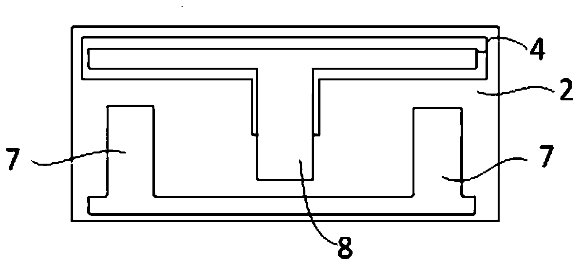
[0050] This embodiment provides a display body. On the basis of the first embodiment above, the electrode lead region 6 is disposed near one end of the substrate 1 , and the electrode lead region 6 is disposed opposite to the groove 4 . Such as image 3 As shown, the anode lead region 9 is arranged on both sides of the electrode lead region 6 , and the cathode lead region 10 is arranged in the middle of the electrode lead region 6 . Optionally, the cathode lead region 10 is located at the central axis of the electrode lead region 6 .
[0051] Further, such as figure 2 As shown, two anode conductive coatings 7 and one cathode conductive coating 8 are arranged in the groove 4 or on the top of the groove. Optionally, the two anode conductive coatings 7 are correspondingly connected to two anode lead regions 9 , and the cathode conductive coating 8 is connected to the cathode lead region 10 . Optionally, the anode conductive coating 7 or the cathode conductive coating 8 has an...
Embodiment 3
[0054] This embodiment provides a display body, on the basis of the above-mentioned embodiments 1 and 2, such as Figure 4 As shown, the display screen body 14 includes at least two, and the exterior of the display screen body 14 is respectively provided with an anode conductive point 12 and a cathode conductive point 11, and the anode conductive point 12 is connected to the anode lead area 9 and an external power supply 13, the cathode conductive point 11 connects the cathode lead area 10 and the negative pole of the external power supply 13.
[0055] Further, when the OLED large substrate contains a plurality of the above-mentioned display screen bodies 14, the multiple display screen bodies 14 are arranged in a matrix on the large substrate, and on both sides of the row direction, a plurality of display screen bodies 14 are arranged outside the display screen body 14. An anode conductive point 12 and a cathode conductive point 11, each anode conductive point 12 is connected...
PUM
 Abstract
Description
Claims
Application Information
 - R&D
- Intellectual Property
- Life Sciences
- Materials
- Tech Scout
- Unparalleled Data Quality
- Higher Quality Content
- 60% Fewer Hallucinations
Browse by: Latest US Patents, China's latest patents, Technical Efficacy Thesaurus, Application Domain, Technology Topic, Popular Technical Reports.
© 2025 PatSnap. All rights reserved.Legal|Privacy policy|Modern Slavery Act Transparency Statement|Sitemap|About US| Contact US: help@patsnap.com


