chip transfer method

A chip transfer and chip technology, applied in the direction of semiconductor devices, electrical components, circuits, etc., can solve the problems of high production cost and low transfer efficiency, and achieve the effect of improving transfer efficiency, realizing density adjustment, and reducing transfer cost.

Active Publication Date: 2022-03-15
SHENZHEN SITAN TECH CO LTD
View PDF3 Cites 0 Cited by
  • Summary
  • Abstract
  • Description
  • Claims
  • Application Information

AI Technical Summary

Problems solved by technology

[0003] Transfer is a key technology in the field of Micro-LED chips. The traditional transfer method is generally: cutting a large number of Micro-LED chips on the ready-made chip board one by one, and then transfer them one by one (or dozens of them together) to the target part. , the transfer efficiency is low, the production cost is high, and it is not suitable for the preparation process of high-precision display screens

Method used


Image

  • chip transfer method
  • chip transfer method
  • chip transfer method

Examples


Embodiment 1

[0047] figure 1 A flow chart of a chip transfer method provided by Embodiment 1 of the present invention specifically includes the following steps:

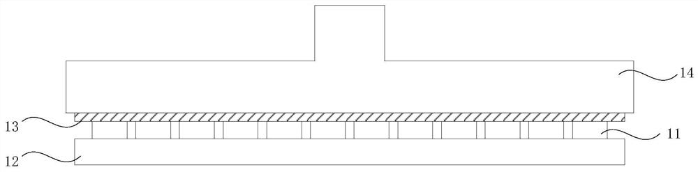
[0048] Step 110, covering the first side of the at least two chips to be transferred with the first surface of the elastic film to absorb the at least two chips to be transferred with a first distance, the first surface of the elastic film is coated with Adhesive layer;

[0049] In this embodiment, the adhesive layer coated on the first surface of the elastic film is used to absorb at least two chips to be transferred. The first spacing is the spacing between two adjacent chips, which may be the original spacing after the wafer is cut, or the spacing between two adjacent chips after at least two chips to be transferred have been rearranged.

[0050] After covering the first surface of the elastic film on the first sides of at least two chips to be transferred, it also includes: pressing the second surface of the elastic film by...

Embodiment 2

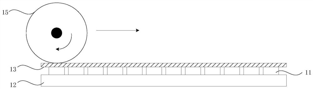
[0092] Figure 9 A flow chart of a chip transfer method provided by Embodiment 1 of the present invention specifically includes the following steps:

[0093] Step 210, covering the first surface of the elastic film on the first side of at least two chips to be transferred according to the first position mark, so as to absorb the at least two chips to be transferred with a first distance, the elastic film The first surface of the elastic film is coated with an adhesive layer, and the elastic film is provided with a first position mark;

[0094] In this embodiment, the adhesive layer coated on the first surface of the elastic film is used to absorb at least two chips to be transferred. The first spacing is the spacing between two adjacent chips, which may be the original spacing after the wafer is cut, or the spacing between two adjacent chips after at least two chips to be transferred have been rearranged. The first position mark is arranged on the elastic film, and may be a ...


PUM


Abstract

The invention discloses a chip transfer method, comprising: covering the first surface of an elastic film on the first side of at least two chips to be transferred to absorb the at least two chips to be transferred with a first distance, the The first surface of the elastic film is coated with an adhesive layer; the elastic film is stretched in at least one direction to adjust the distance between the at least two chips to be transferred as the second distance; the stretched elastic The first surface of the film covers the target piece to transfer the at least two chips to be transferred to the target piece with the second distance. It solves the problem of mass transfer of existing chips, realizes the effect of improving transfer efficiency and reducing transfer cost, and also realizes density adjustment during chip transfer.

Description

technical field [0001] The embodiment of the present invention relates to a chip transfer technology, in particular to a chip transfer method. Background technique [0002] Micro-LED is a new generation of display technology, which has higher brightness and better luminous efficiency than the existing OLED technology, but lower power consumption. Micro-LED has a series of advantages, and it is foreseeable that it will be widely used in the field of display technology in the future. [0003] Transfer is a key technology in the field of Micro-LED chips. The traditional transfer method is generally: cutting a large number of Micro-LED chips on the ready-made chip board one by one, and then transfer them one by one (or dozens of them together) to the target part. , the transfer efficiency is low, the production cost is high, and it is not suitable for the preparation process of high-precision display screens. Contents of the invention [0004] The invention provides a chip t...

Claims


Application Information

Patent Timeline
Patent Type & Authority Patents(China)
IPC IPC(8): H01L21/67H01L33/48
CPCH01L21/67092H01L21/67144H01L33/48H01L2933/0033
Inventor 刘召军邱成峰莫炜静郑汉宇
Owner SHENZHEN SITAN TECH CO LTD
Why Eureka
Try Eureka