Ytterbium-thulium doped strontium titanate semiconductor material as well as preparation method and application thereof
A strontium titanate and semiconductor technology, applied in the field of thulium strontium titanate semiconductor materials and its preparation, and doping with ytterbium, can solve the problems of difficult infrared light utilization, achieve good repeatability, improve efficiency, and good ultraviolet-infrared absorption Effect
- Summary
- Abstract
- Description
- Claims
- Application Information
AI Technical Summary
Problems solved by technology
Method used
Image

Examples
Embodiment 1
[0048] Example 1: SrTiO 3 : Preparation of Yb, Tm.
[0049] (1) 319.32mg TiO 2 , 584.5752mg SrCO 3 , 13.6mg Yb 2 o 3 , 0.96415mg Tm 2 o 3 (according to SrTiO 3 :Yb 3+ ,Tm 3+ Mole ratio 99:8 / 9:1 / 9 ratio) into the agate mortar.
[0050] (2) Add 7.4436 g of NaCl to the agate mortar of step (1), grind in cis for 20 minutes, and mix the raw materials evenly.
[0051] (3) Transfer the homogeneously mixed raw materials in step (2) to a platinum pot and compact them.
[0052] (4) Put the platinum pot in step (3) into a tube furnace, and calcinate at 1000° C. for 3 hours.
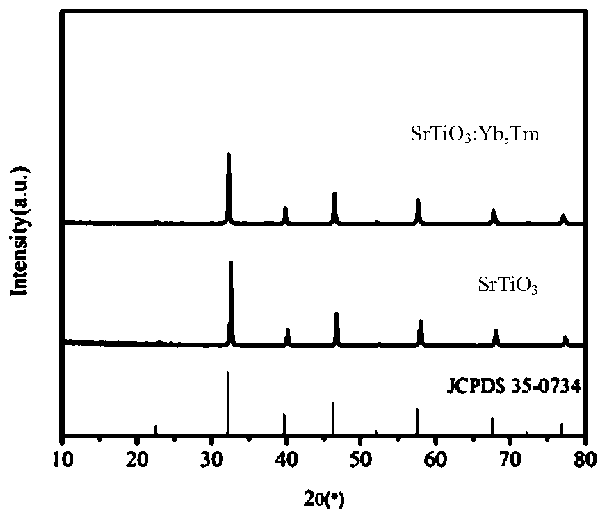
[0053] (5) After the sample calcined in step (4) was cooled to room temperature by the tube furnace program, it was taken out, ultrasonically cleaned 6 times with deionized water, centrifuged, and dried overnight in an oven at 60°C to obtain SrTiO 3 : Yb, Tm. The X-ray diffraction pattern of the sample is as figure 1 shown, without Yb 2 o 3 、Tm 2 o 3 The characteristic peak appears, indicating tha...
Embodiment 2
[0055] (1) 319.32mg TiO 2 , 584.5752mg SrCO 3 , 13.6mg Yb 2 o 3 , 0.96415mg Tm 2 o 3 (according to SrTiO 3 :Yb 3+ ,Tm 3+ Mole ratio 99:8 / 9:1 / 9 ratio) into the agate mortar.
[0056] (2) Add 7.4436 g of NaCl to the agate mortar of step (1), grind in cis for 20 minutes, and mix the raw materials evenly.
[0057] (3) Transfer the homogeneously mixed raw materials in step (2) to a platinum pot and compact them.
[0058] (4) Put the platinum pot in step (3) into a tube furnace, and calcinate at 900° C. for 3 hours.
[0059] (5) The sample calcined in step (4) was cooled to room temperature in a tube furnace program, then taken out, ultrasonically cleaned 6 times with deionized water, centrifuged, and dried overnight in an oven at 60°C to obtain a solid material. After the sample is irradiated with a 980nm laser, it does not emit light, indicating that the reaction temperature has not been reached, and the doping has failed.
Embodiment 3
[0061] (1) 319.32mg TiO 2 , 584.5752mg SrCO 3 , 351.12528mg Yb 2 o 3 、38.2mg Tm 2 o 3 (according to SrTiO 3 :Yb 3+ ,Tm 3+ Mole ratio 80:18:2 ratio) into the agate mortar.
[0062] (2) Add 7.4436 g of NaCl to the agate mortar of step (1), grind in cis for 20 minutes, and mix the raw materials evenly.
[0063] (3) Transfer the homogeneously mixed raw materials in step (2) to a platinum pot and compact them.
[0064] (4) Put the platinum pot in step (3) into a tube furnace, and calcinate at 1000° C. for 3 hours.
[0065] (5) The sample calcined in step (4) was cooled to room temperature in a tube furnace program, then taken out, ultrasonically cleaned 6 times with deionized water, centrifuged, and dried overnight in an oven at 60°C to obtain a solid material. The X-ray diffraction pattern of the sample is as Image 6 As shown in , there are miscellaneous peaks, indicating that the doping has not been successful and is not the target product.
PUM
| Property | Measurement | Unit |
|---|---|---|
| particle diameter | aaaaa | aaaaa |
Abstract
Description
Claims
Application Information
 - Generate Ideas
- Intellectual Property
- Life Sciences
- Materials
- Tech Scout
- Unparalleled Data Quality
- Higher Quality Content
- 60% Fewer Hallucinations
Browse by: Latest US Patents, China's latest patents, Technical Efficacy Thesaurus, Application Domain, Technology Topic, Popular Technical Reports.
© 2025 PatSnap. All rights reserved.Legal|Privacy policy|Modern Slavery Act Transparency Statement|Sitemap|About US| Contact US: help@patsnap.com