A Polarization-Independent Ultranarrow Multiband Tunable Perfect Absorber
A multi-band absorber technology, applied in the field of optical characteristics, can solve the problems of fixed bandwidth operating frequency, limit the application range of metamaterial absorbers, single operating frequency band, etc., and achieve the effects of high sensitivity, simple structure, and easy manufacture
- Summary
- Abstract
- Description
- Claims
- Application Information
AI Technical Summary
Problems solved by technology
Method used
Image
Examples
Embodiment 1
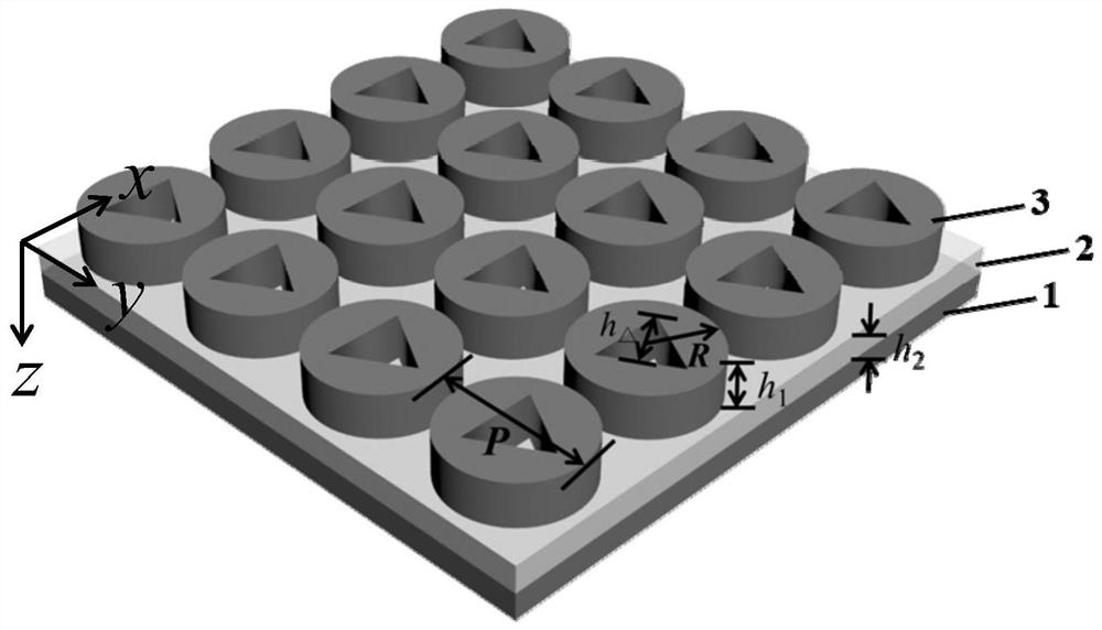
[0038] A polarization-independent ultra-narrow multi-band tunable perfect absorber, from bottom to top:
[0039] A gold layer having a thickness of 100 nanometers;
[0040] a layer of silicon dioxide disposed on the gold layer having a thickness of 120 nanometers;
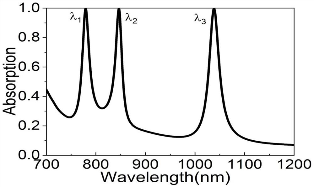
[0041] The periodic gold nanostructure array layer arranged on the silicon dioxide layer includes several gold nano cylinders arranged with a period of 600 nanometers, the radius (R) of each gold nano cylinder is 210 nanometers, and each gold nano cylinder Etching has triangular prism air hole in the body; The center of the equilateral triangle of the bottom surface of the triangular prism air hole overlaps with the center of the circular bottom surface of the gold nano cylinder, and the height (h △ ) is 180 nm, the height of triangular prism air holes and gold nanocylinders (h 1 ) are all 30 nanometers.
[0042] figure 2 Triple-band absorption spectrum plot of the polarization-independent ultranarrow multiban...
Embodiment 2
[0044] A polarization-independent ultra-narrow multi-band tunable perfect absorber, from bottom to top:
[0045] A gold layer having a thickness of 100 nanometers;
[0046] a layer of silicon dioxide disposed on the gold layer having a thickness of 120 nanometers;
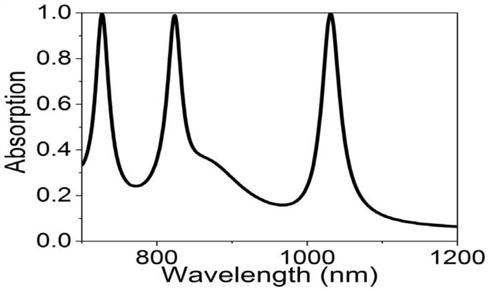
[0047] The periodic gold nanostructure array layer arranged on the silicon dioxide layer includes several gold nano cylinders in a periodic array of 500 nanometers, the radius (R) of each gold nano cylinder is 210 nanometers, and each gold nano cylinder Etching has triangular prism air hole in the body; The center of the equilateral triangle of the bottom surface of the triangular prism air hole overlaps with the center of the circular bottom surface of the gold nano cylinder, and the height (h △ ) is 180 nm, the height of the triangular prism air hole and the gold nano cylinder (h 1 ) are all 30 nanometers.
[0048] image 3 Triple-band absorption spectrum plot of the polarization-independent ultranarrow multiba...
Embodiment 3
[0050] A polarization-independent ultra-narrow multi-band tunable perfect absorber, from bottom to top:
[0051] A gold layer having a thickness of 100 nanometers;
[0052] a layer of silicon dioxide disposed on the gold layer having a thickness of 120 nanometers;
[0053] The periodic gold nanostructure array layer arranged on the silicon dioxide layer includes several gold nano cylinders in a periodic array of 600 nanometers, the radius (R) of each gold nano cylinder is 210 nanometers, and each gold nano cylinder Etching has triangular prism air hole in the body; The center of the equilateral triangle of the bottom surface of the triangular prism air hole overlaps with the center of the circular bottom surface of the gold nano cylinder, and the height (h △ ) is 195 nanometers, the height of triangular prism air holes and gold nano cylinders (h 1 ) are all 30 nanometers.
[0054] Figure 4 Triple-band absorption spectrum plot of the polarization-independent ultranarrow mu...
PUM
| Property | Measurement | Unit |
|---|---|---|
| thickness | aaaaa | aaaaa |
| radius | aaaaa | aaaaa |
| height | aaaaa | aaaaa |
Abstract
Description
Claims
Application Information
 - Generate Ideas
- Intellectual Property
- Life Sciences
- Materials
- Tech Scout
- Unparalleled Data Quality
- Higher Quality Content
- 60% Fewer Hallucinations
Browse by: Latest US Patents, China's latest patents, Technical Efficacy Thesaurus, Application Domain, Technology Topic, Popular Technical Reports.
© 2025 PatSnap. All rights reserved.Legal|Privacy policy|Modern Slavery Act Transparency Statement|Sitemap|About US| Contact US: help@patsnap.com


