
Silicon wafer surface treatment method for graphene in-situ growth

An in-situ growth, silicon wafer surface technology, used in electrical components, semiconductor/solid-state device manufacturing, circuits, etc., to achieve the effect of improving capacity, helping mass production, and repeating the method

Inactive Publication Date: 2019-10-15
ZHEJIANG UNIV
View PDF2 Cites 0 Cited by
  • Summary
  • Abstract
  • Description
  • Claims
  • Application Information

AI Technical Summary

Problems solved by technology

However, until now, large-area graphene preparation on silicon substrates has not been reported. The core difficulty lies in breaking through the self-limitation of graphene growth on the silicon surface.

Method used


Image

  • Silicon wafer surface treatment method for graphene in-situ growth
  • Silicon wafer surface treatment method for graphene in-situ growth
  • Silicon wafer surface treatment method for graphene in-situ growth

Examples


Embodiment 1

[0035] The silicon chip surface treatment method that is used for graphene in-situ growth of the present embodiment specifically comprises the following steps:

[0036] (1) Take (100) silicon wafers for growth, place them in deionized water for simple ultrasonic cleaning for 1 min, and then immerse in dilute hydrofluoric acid with a volume ratio of 1:100 for 1 min;

[0037] (2) Take out the silicon wafer, rinse the surface with deionized water, and dry it with 0.5MPa high-pressure nitrogen;

[0038] (3) Immerse the silicon wafer in 0.1M p-diphenol methanol solution for 1 hour;

[0039] (4) Take out the silicon chip and rinse it three times with absolute ethanol solution;

[0040] (5) After rinsing, the silicon wafer was blown dry with 0.5MPa high-pressure nitrogen, placed in a tube furnace, and grown graphene by chemical vapor deposition for 30 minutes to obtain a large number of graphene crystal nuclei.

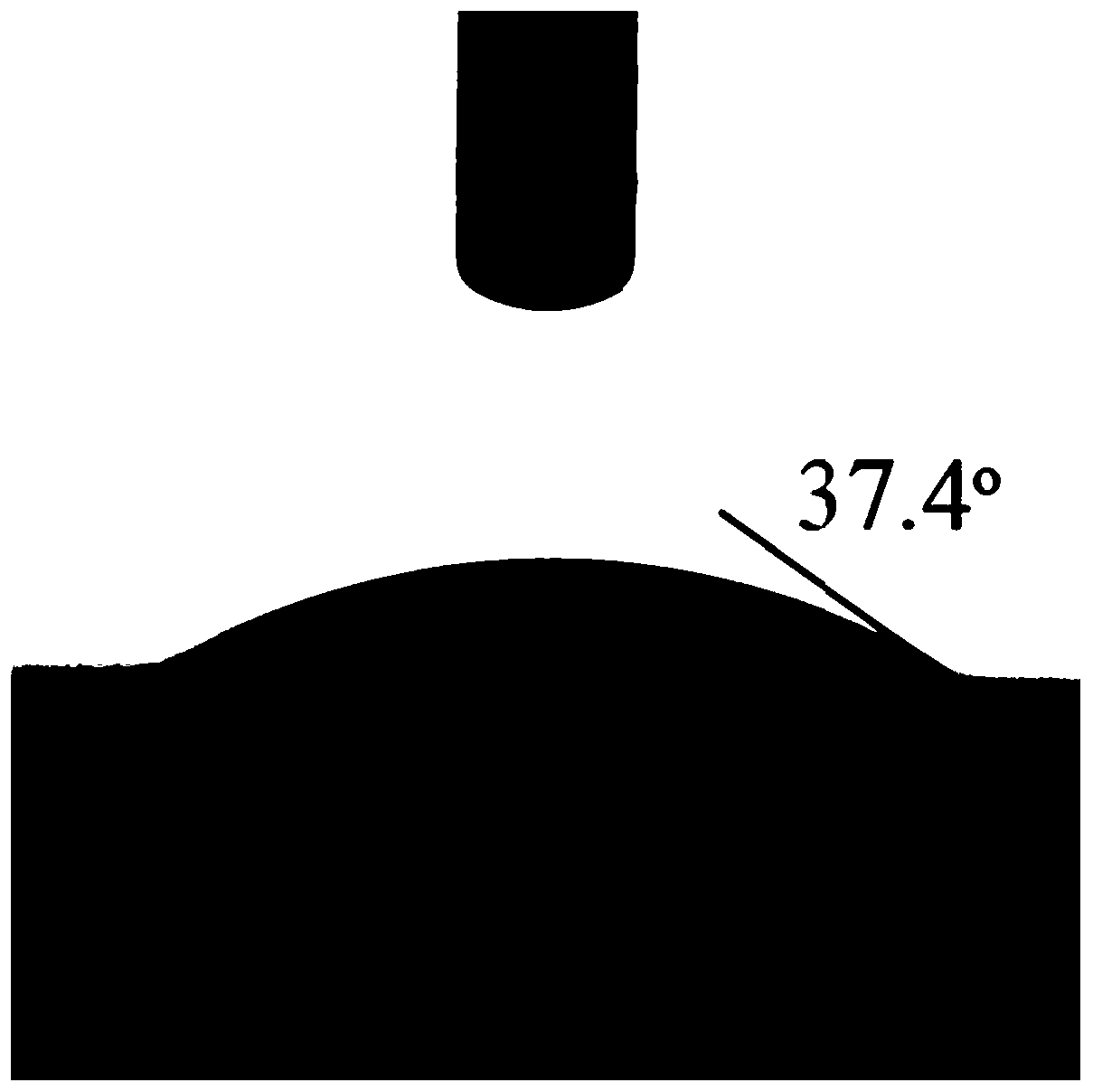
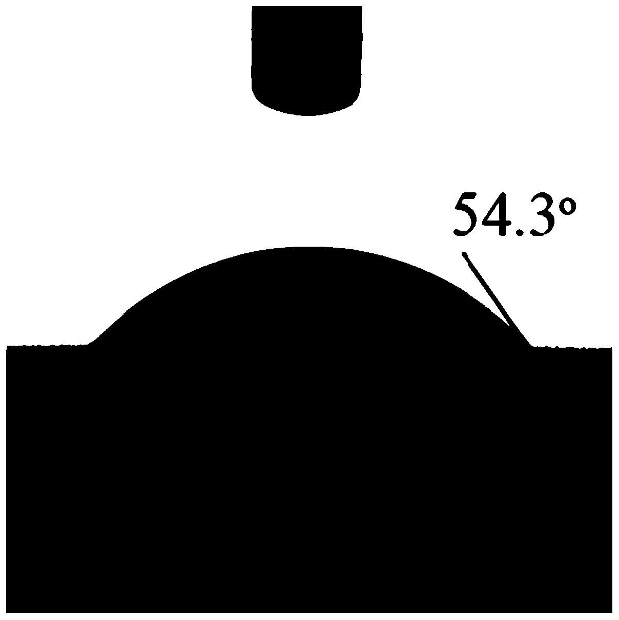
[0041] The water contact angle measuring instrument was used to chara...

Embodiment 2

[0046] The silicon chip surface treatment method that is used for graphene in-situ growth of the present embodiment specifically comprises the following steps:

[0047] (1) Take (100) silicon wafers for growth, place them in deionized water for simple ultrasonic cleaning for 1 min, and then immerse in dilute hydrofluoric acid with a volume ratio of 1:50 for 1 min;

[0048] (2) Take out the silicon wafer, rinse the surface with deionized water, and dry it with 0.5MPa argon;

[0049] (3) Immerse the silicon wafer in 0.1M phenol-methanol solution for 1 hour;

[0050] (4) Take out the silicon chip and rinse it three times with absolute ethanol solution;

[0051] (5) After rinsing, the silicon wafer was blown dry with 0.5 MPa argon gas for the preparation of graphene.

Embodiment 3

[0053] The silicon chip surface treatment method that is used for graphene in-situ growth of the present embodiment specifically comprises the following steps:

[0054] (1) Take the (111) silicon wafer for growth, place it in deionized water for simple ultrasonic cleaning for 1 min, and then immerse it in dilute hydrofluoric acid with a volume ratio of 1:30 for 1 min;

[0055] (2) Take out the silicon wafer, rinse the surface with deionized water, and dry it with 1MPa argon;

[0056] (3) Immerse the silicon wafer in 0.2M resorcinol methanol solution for 30min;

[0057] (4) Take out the silicon chip and rinse it three times with absolute ethanol solution;

[0058] (5) After rinsing, the silicon wafer was blown dry with 1 MPa argon gas for the preparation of graphene.


PUM


Abstract

The invention discloses a silicon wafer surface treatment method for graphene in-situ growth. The silicon wafer surface treatment method comprises the steps of: (1) immersing a clean silicon wafer into a hydrofluoric acid aqueous solution, then taking out the silicon wafer, washing the silicon wafer with deionized water, and performing drying; and (2) soaking the dried silicon wafer into an alcohol solution of a phenol derivative, then taking out the silicon wafer, rinsing the silicon wafer by using an anhydrous alcohol solvent, and drying the silicon wafer to obtain the silicon wafer for graphene in-situ growth. According to the invention, the phenol derivative is used for passivating dangling bonds on the surface of the clean silicon, so that the contact angle of the surface of the silicon wafer is reduced, a nucleation site is provided for the growth of graphene, and the treated silicon substrate can be used for preparing large-area graphene in situ. The method has the simple process and the obvious effect.

Description

technical field [0001] The invention relates to the technical field of preparation of graphene functional materials, in particular to a silicon chip surface treatment method for in-situ growth of graphene. Background technique [0002] Graphene is a two-dimensional atomic crystal with densely connected carbon atoms through conjugation and a hexagonal honeycomb structure. As a typical two-dimensional crystal, graphene has properties unmatched by other conventional materials in terms of electrical conductivity, thermal conductivity and strength. Its inherent high light transmittance and high electrical conductivity make graphene have great application prospects in transparent electrodes, displays, and photovoltaic devices. The special properties brought about by its two-dimensional structure, such as quantum Hall effect, topological insulation, low-temperature superconductivity, etc., make graphene also occupy an important position in new electronic components in the future. ...

Claims


Application Information

Patent Timeline
Patent Type & Authority Applications(China)
IPC IPC(8): H01L21/02
CPCH01L21/02381H01L21/02527H01L21/02658H01L21/02661
Inventor 余学功黄琨丛靖昆杨德仁
Owner ZHEJIANG UNIV
Learn More