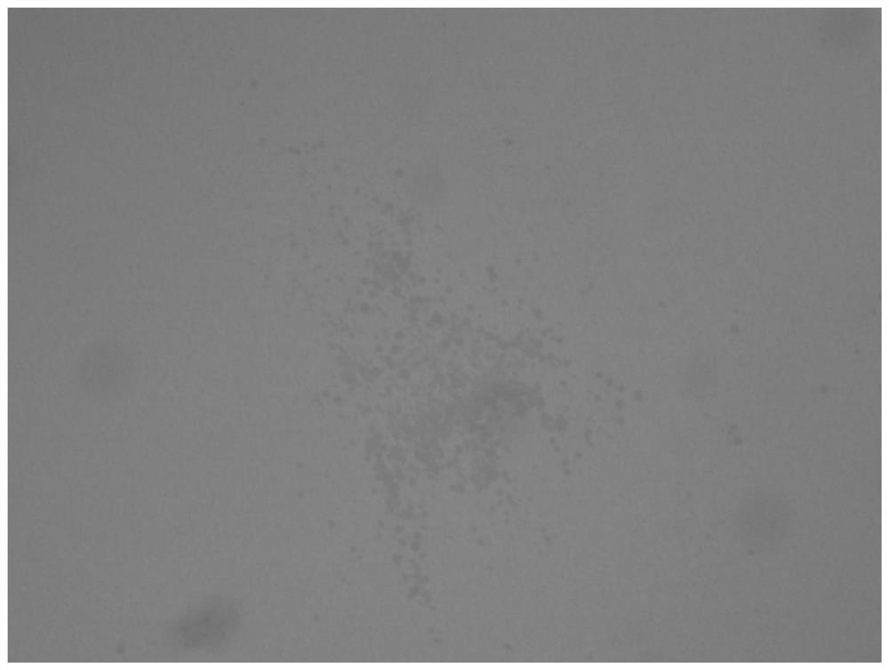
A method for suppressing the formation of carbon inclusion defects in the growth of conductive silicon carbide crystals
A technology of crystal growth and silicon carbide, which is applied in crystal growth, single crystal growth, single crystal growth, etc., can solve problems such as carbon inclusions, avoid the formation of carbon inclusions, reduce the excess of C sources, and inhibit The effect produced
- Summary
- Abstract
- Description
- Claims
- Application Information
AI Technical Summary
Problems solved by technology
Method used
Image
Examples
Embodiment 1
[0037] A method for suppressing the generation of carbon inclusion defects in the growth of conductive silicon carbide crystals:
[0038] Step a, mixing carbon powder and silicon powder evenly according to the molar ratio of 1:1, the purity of both is ≥5N, and the particle size is <100 μm;
[0039] Step b, put uniformly mixed carbon powder and silicon powder into a high-purity graphite crucible, place the graphite crucible in an induction-heated synthesis furnace, evacuate to a pressure <1E-5Torr, discharge the air from the reaction chamber, and heat To 1100°C, feed a mixed gas of high-purity argon and nitrogen into the reaction chamber until the pressure is 10Torr, the volume content of nitrogen in the reaction chamber is 4%, gradually increase the temperature to 2100°C at a rate of 100°C / h, and react for 12 hours , feed protective gas to a pressure of 600 Torr, cool down, and obtain nitrogen-containing silicon carbide powder;
[0040] Step c, to put the nitrogen-containing ...
Embodiment 2
[0042] A method for suppressing the generation of carbon inclusion defects in the growth of conductive silicon carbide crystals:
[0043] Step a, mixing carbon powder and silicon powder evenly according to the molar ratio of 1:1.01, the purity of both is ≥5N, and the particle size is <100 μm;
[0044] Step b, put uniformly mixed carbon powder and silicon powder into a high-purity graphite crucible, place the graphite crucible in an induction-heated synthesis furnace, evacuate to a pressure <1E-5Torr, discharge the air from the reaction chamber, and heat To 1000°C, feed a mixed gas of high-purity argon and nitrogen into the reaction chamber until the pressure is 1Torr, the volume content of nitrogen in the reaction chamber is 3%, gradually increase the temperature to 2000°C at a rate of 90°C / h, and react for 10h , feed protective gas to a pressure of 500 Torr, lower the temperature, and obtain nitrogen-containing silicon carbide powder;
[0045] Step c, to put the nitrogen-con...
Embodiment 3
[0047] A method for suppressing the generation of carbon inclusion defects in the growth of conductive silicon carbide crystals:
[0048] Step a, mixing carbon powder and silicon powder evenly according to the molar ratio of 1:1.02, the purity of both is ≥5N, and the particle size is <100 μm;
[0049] Step b, put uniformly mixed carbon powder and silicon powder into a high-purity graphite crucible, place the graphite crucible in an induction-heated synthesis furnace, evacuate to a pressure <1E-5Torr, discharge the air from the reaction chamber, and heat To 1050°C, feed a mixture of high-purity argon and nitrogen into the reaction chamber until the pressure is 20 Torr, the volume content of nitrogen in the reaction chamber is 6%, gradually increase the temperature to 2200°C at a rate of 120°C / h, and react for 15 hours , feed protective gas to a pressure of 400 Torr, cool down, and obtain nitrogen-containing silicon carbide powder;
[0050] Step c, to put the nitrogen-containin...
PUM
| Property | Measurement | Unit |
|---|---|---|
| purity | aaaaa | aaaaa |
Abstract
Description
Claims
Application Information
 - R&D
- Intellectual Property
- Life Sciences
- Materials
- Tech Scout
- Unparalleled Data Quality
- Higher Quality Content
- 60% Fewer Hallucinations
Browse by: Latest US Patents, China's latest patents, Technical Efficacy Thesaurus, Application Domain, Technology Topic, Popular Technical Reports.
© 2025 PatSnap. All rights reserved.Legal|Privacy policy|Modern Slavery Act Transparency Statement|Sitemap|About US| Contact US: help@patsnap.com


