
Gate drive current charging circuit and gate drive control circuit of power device

A charging circuit and power device technology, which is applied in the direction of control/regulation systems, instruments, and adjustment of electrical variables, etc., can solve problems such as low flexibility, low reliability, and low adjustment accuracy

Active Publication Date: 2019-09-17
UNIV OF ELECTRONICS SCI & TECH OF CHINA
View PDF4 Cites 11 Cited by
  • Summary
  • Abstract
  • Description
  • Claims
  • Application Information

AI Technical Summary

Problems solved by technology

[0005] In view of the problems of low adjustment accuracy, unsuitable for integrated packaging applications, introduction of gate parasitic inductance, low reliability and low flexibility in high-voltage applications in the above-mentioned method of adjusting the gate drive current intensity by changing the resistance value of the series resistor, The present invention proposes a gate drive current charging circuit for a power device and a gate drive control circuit for a power device. The gate drive control circuit uses an adjustable current source instead of a series resistor to provide a charging current for the power device. By adjusting the adjustable current source The magnitude of the current changes the dv / dt slope of the SW point to adjust the EMI (electromagnetic interference) of the system. It has the characteristics of high precision and high flexibility, and when the gate voltage of the power device reaches the logic relatively high level of the gate drive control circuit Stop generating the charging current, and no additional power consumption will be generated; the gate drive current charging circuit of the power device proposed by the present invention is actually an adjustable current source with a maximum current clamp, which is changed by adjusting the current value generated by the adjustable current source. Power device gate charging intensity, setting the maximum current clamp can improve system reliability

Method used


Image

  • Gate drive current charging circuit and gate drive control circuit of power device
  • Gate drive current charging circuit and gate drive control circuit of power device
  • Gate drive current charging circuit and gate drive control circuit of power device

Examples


Embodiment Construction

[0054] The present invention will be described in detail below in conjunction with the accompanying drawings and specific embodiments.

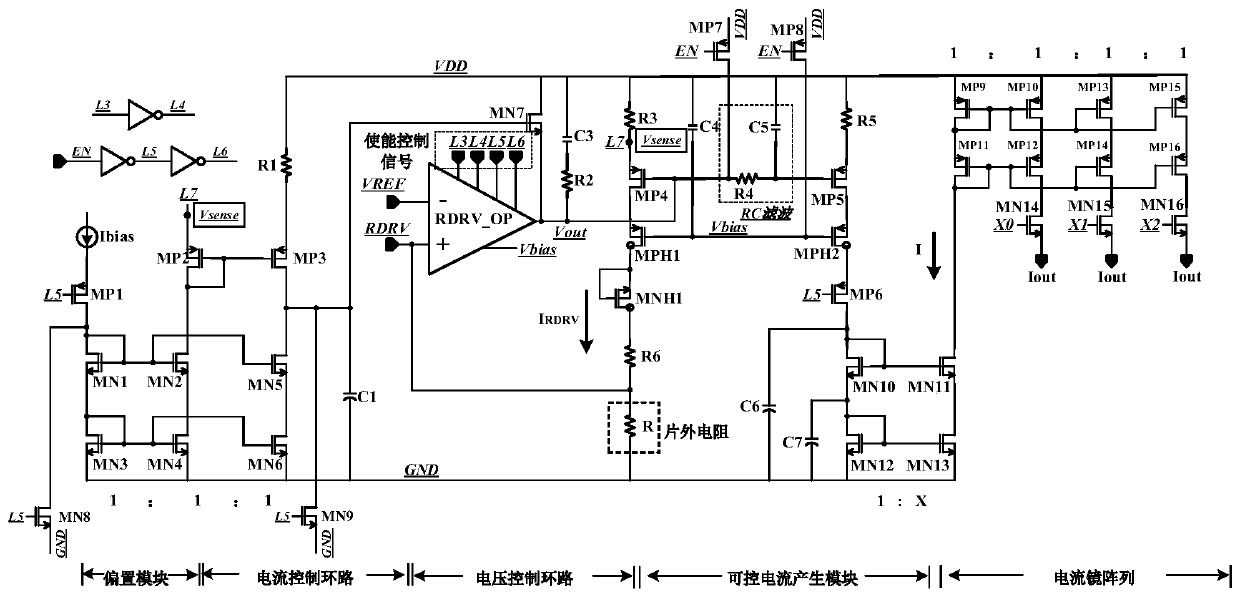
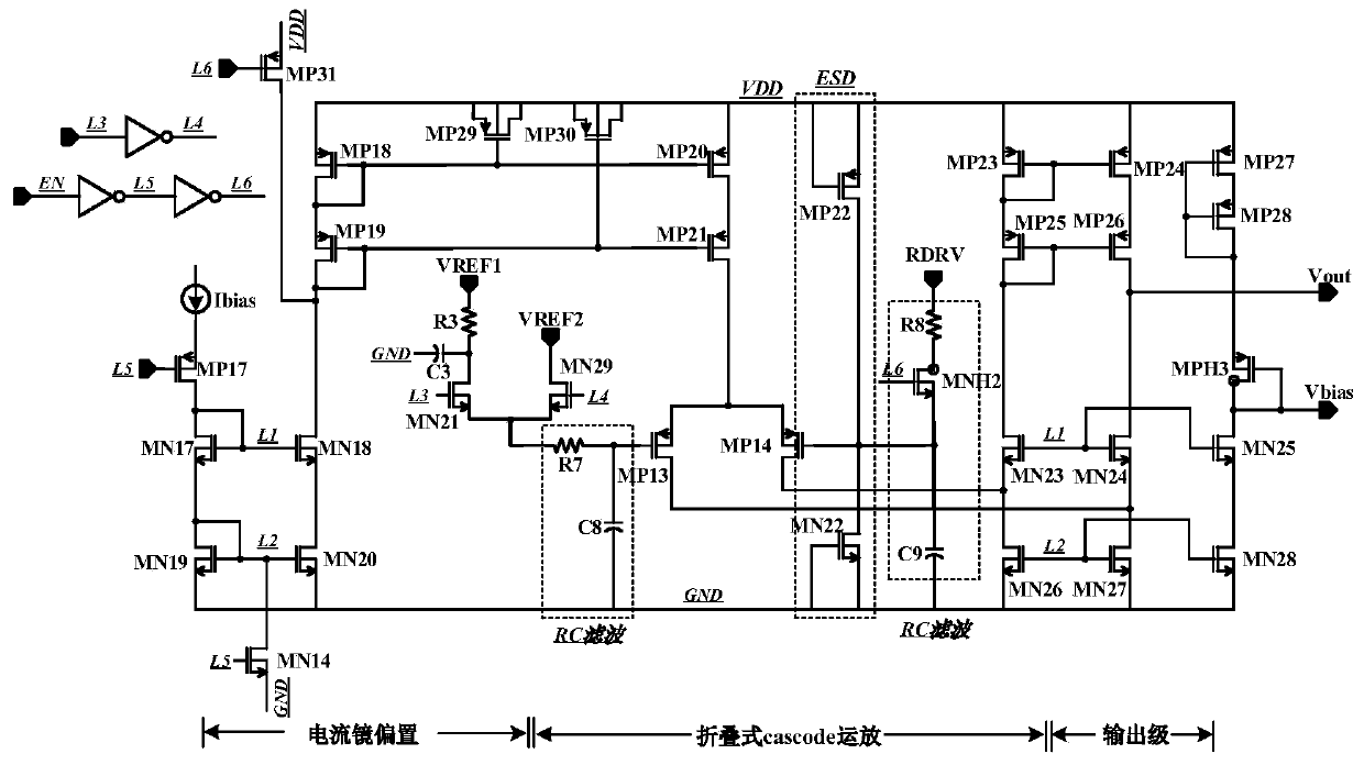
[0055] Such as figure 2 Shown is the gate drive current charging circuit of the power device proposed by the present invention. In this embodiment, the charging circuit is applied to the low-side power device, and its power rail is VDD-GND. The charging circuit is actually a maximum current clamp The on-chip adjustable current source circuit includes an off-chip resistor R, a bias module, a current control loop, a voltage control loop, a controllable current generation module and a current mirror array. The bias module is used to generate the first bias voltage and the second bias voltage, such as figure 2 The figure shows an implementation form of the bias module, including the first PMOS transistor MP1, the first NMOS transistor MN1, the third NMOS transistor MN3 and the eighth NMOS transistor MN8, the source of the first PMOS transistor...


PUM


Abstract

The invention provides a gate drive current charging circuit of a power device and a gate drive control circuit of the power device. The gate drive control circuit separates charge and discharge paths, and uses an adjustable current source to provide charging current for the power device, with more flexible and reliable control mode, which can be applicable to integrated package applications of the power device, especially for depletion-type GaN power transistors. The gate drive current charging circuit is an on-chip adjustable current source with maximum current clamp, and the generated charging current is adjusted by adjusting the voltage value of the reference voltage, the resistance value of the off-chip resistor and the number of strobe current mirror units, so as to ensure more flexible and accurate control of the charging current of the power device. A current control loop is used to realize the maximum current clamping, and a filtering structure is set to eliminate the influence of noise, so as to improve the system reliability. At the same time, when the gate voltage of the power device reaches the logic high level of the gate drive control circuit, the generation of the charging current is stopped, and no additional power consumption is generated. No series resistance is used, so that no gate parasitic inductance is introduced.

Description

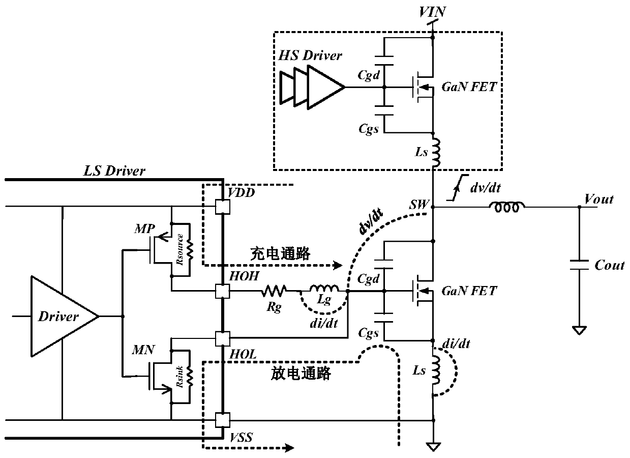
technical field [0001] The invention belongs to the technical field of electronic circuits, and in particular relates to a charging circuit for providing charging current for a power device gate drive current, and a power device gate drive control circuit for charging by using an adjustable current source. Background technique [0002] In recent years, Si-based GaN power devices have gradually become a research hotspot in the field of power management, and are expected to replace Si MOS power transistors as future high-performance power system solutions. Therefore, the design of a high-efficiency and high-reliability GaN power device half-bridge gate drive circuit design is very critical. [0003] figure 1 Shown is a traditional GaN half-bridge drive circuit diagram. In the figure, only the drive stage circuit of the low-side circuit is specifically drawn, and the drive stage of the high-side circuit is the same as the low-side circuit. Since the capacitance and inductance...

Claims


Application Information

Patent Timeline
Patent Type & Authority Applications(China)
IPC IPC(8): G05F1/575
CPCG05F1/575
Inventor 明鑫冯旭东许齐飞毛帅王卓张波
Owner UNIV OF ELECTRONICS SCI & TECH OF CHINA
Learn More