Defect detection method of metal silicide and formation method of semiconductor structure

A technology of metal silicide and metal silicide layer, which is used in semiconductor/solid-state device manufacturing, semiconductor/solid-state device testing/measurement, electrical components, etc. The effect of batch defective products, reducing the cost and time of inspection

Active Publication Date: 2019-08-27
WUHAN XINXIN SEMICON MFG CO LTD
View PDF5 Cites 3 Cited by
  • Summary
  • Abstract
  • Description
  • Claims
  • Application Information

AI Technical Summary

Problems solved by technology

[0004] The object of the present invention is to provide a metal silicide defect detection method and a method for forming a semiconductor structure, so as to solve the problem of low detection accuracy of existing metal silicide defects

Method used


Image

  • Defect detection method of metal silicide and formation method of semiconductor structure
  • Defect detection method of metal silicide and formation method of semiconductor structure
  • Defect detection method of metal silicide and formation method of semiconductor structure

Examples


Embodiment Construction

[0043] The specific implementation manner of the present invention will be described in more detail below with reference to schematic diagrams. The advantages and features of the present invention will be more apparent from the following description. It should be noted that all the drawings are in a very simplified form and use imprecise scales, and are only used to facilitate and clearly assist the purpose of illustrating the embodiments of the present invention.

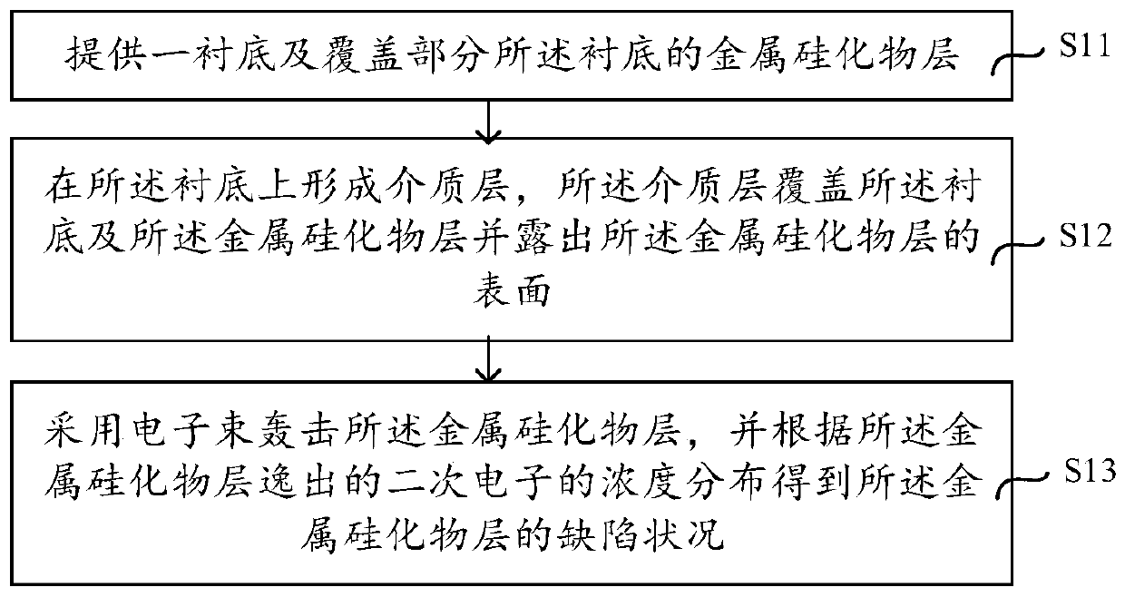
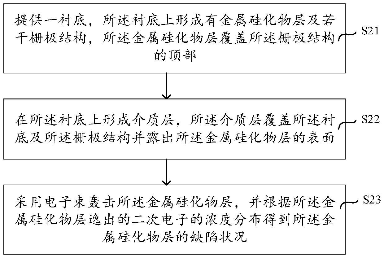
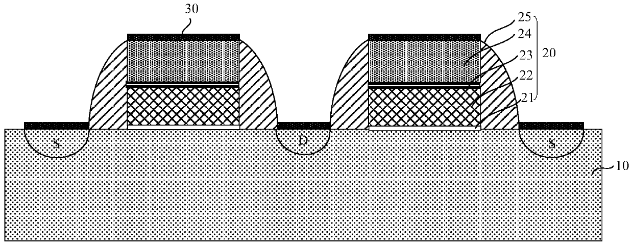
[0044] Such as figure 1 As shown, this embodiment provides a method for detecting defects in metal silicides, including:

[0045] S11: providing a substrate and a metal silicide layer covering part of the substrate;

[0046] S21: forming a dielectric layer on the substrate, the dielectric layer covering the substrate and the metal silicide layer and exposing the surface of the metal silicide layer;

[0047] S31: Bombarding the metal silicide layer with an electron beam, and obtaining defect conditions of the met...


PUM


Abstract

The invention provides a defect detection method of a metal silicide and a formation method of a semiconductor structure. The defect detection method comprises the following steps: providing a substrate and a metal silicide layer with which a part of the substrate is covered; then forming a dielectric layer on the substrate, wherein the substrate and the metal silicide layer are covered with the dielectric layer and the surface of the metal silicide layer is exposed so that the areas except the metal silicide layer are insulated respectively; then, bombarding the metal silicide layer with an electron beam, and obtaining the defect condition of the metal silicide layer according to the concentration distribution of secondary electrons escaped from the metal silicide layer. Therefore, quantitative detection can be carried out on the defects of the metal silicide layer, the defect detection precision is improved, moreover, the defect detection method of the metal silicide is carried out in the formation process of the semiconductor structure, the defect condition of the metal silicide can be reflected in real time online, normal preparation process of the semiconductor device cannot be disturbed, an extra working procedure cannot be added, and the detection cost and time can be reduced.

Description

technical field [0001] The invention relates to the technical field of semiconductor preparation, in particular to a method for detecting defects of a metal silicide and a method for forming a semiconductor structure. Background technique [0002] A metal silicide is a thermally stable metal compound formed by reacting a transition metal with silicon. Since the metal silicide exhibits the advantages of low resistivity and high thermal stability, and is especially suitable for the current silicon process, the metal silicide has been widely used in the semiconductor device process. Specifically, the metal silicide layer formed on the surface of the gate electrode and the source / drain region can effectively reduce the specific resistance of the gate electrode and the contact resistance of the source / drain. [0003] However, due to factors such as the grain size of the transition metal or oxide residues on the substrate surface, defects will occur in the growth of metal silicid...

Claims


Application Information

Patent Timeline
IPC IPC(8): H01L21/66H01L21/285
CPCH01L21/28518H01L22/12H01L22/24
Inventor 胡航标周伦潮
Owner WUHAN XINXIN SEMICON MFG CO LTD
Why Eureka
Try Eureka