A control method for a dual-input boost inverter

A control method and inverter technology, which are applied in the direction of converting irreversible DC power input into AC power output, output power conversion devices, electrical components, etc., can solve the problem of low utilization rate of input DC voltage and increased voltage stress of power tubes. , affecting the output power quality and other issues, to achieve the effect of cumbersome design, small switching loss, and small footprint

Active Publication Date: 2020-05-12
ANHUI UNIVERSITY OF TECHNOLOGY
View PDF1 Cites 0 Cited by
  • Summary
  • Abstract
  • Description
  • Claims
  • Application Information

AI Technical Summary

Problems solved by technology

[0003] The traditional bridge inverter has the characteristics of simple topology and low cost, so it is widely used, but the upper and lower switching tubes of the same bridge arm have a shoot-through situation, which reduces the reliability of the system; in order to prevent the occurrence of the shoot-through situation, the drive signal The addition of dead time control has brought the following problems: 1) Low-order harmonics are introduced into the grid-connected system, which affects the output power quality and causes output current waveform distortion; 2) The dead time control causes the switching tube Body diode freewheeling and reverse recovery, resulting in additional conduction and reverse recovery losses of freewheeling; 3) dead time control also limits the realization of high frequency conversion
However, its input DC voltage utilization rate is low, and the maximum output voltage of the bridge arm is only half of the input DC voltage. For high-voltage output occasions, a higher input DC voltage is required, which increases the voltage stress of the power tube. It is necessary to use a withstand voltage Higher-grade power devices, leading to higher costs
[0005] Chinese invention patent application, publication number: CN107834886A; publication date: 2018.03.23; discloses a single-stage boost inverter and its control method. It also solves the complex characteristics of the two-stage circuit. Its shortcoming is that the inverter has greatly changed the full-bridge inverter. The starting point is to realize the boost function of the inverter, but it uses More switching devices increase the volume of the circuit, increase the loss, and reduce the efficiency of the inverter
The above papers all involve step-down inverters, but the application scenarios are limited and cannot meet a wide range of needs

Method used


Image

  • A control method for a dual-input boost inverter
  • A control method for a dual-input boost inverter
  • A control method for a dual-input boost inverter

Examples


Embodiment 1

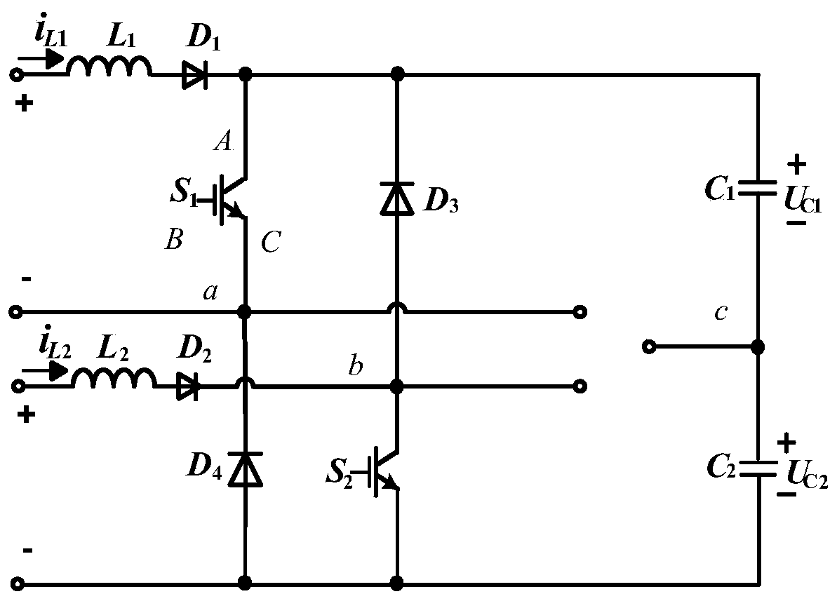
[0057] Such as figure 1 As shown, this embodiment proposes a dual-input boost inverter, including a power switch tube S 1 , S 2 , Diode D 1 、D 2 、D 3 and D 4 , inductance L 1 , L 2 , capacitance C 1 、C 2 ; Among them, one end of the input side is connected to the inductor L 1 One end, the inductance L 1 The other end is connected to the diode D 1 anode connected; diode D 1 The cathodes are respectively connected to the power switch tube S 1 Terminal A, diode D 3 Cathode and Capacitor C 1 One end; input side - the other end, power switch tube S 1 C terminal and diode D 4 The cathode is connected to node a; one end of the input side two is connected to the inductor L 2 One end, the inductance L 2 The other end is connected to the diode D 2 anode connected; diode D 2 Cathode, power switch tube S 2 A terminal and diode D 3 Anode connected to node b; capacitor C 1 The other end is connected to the capacitor C 2 One end of the input side is connected to the n...

Embodiment 2

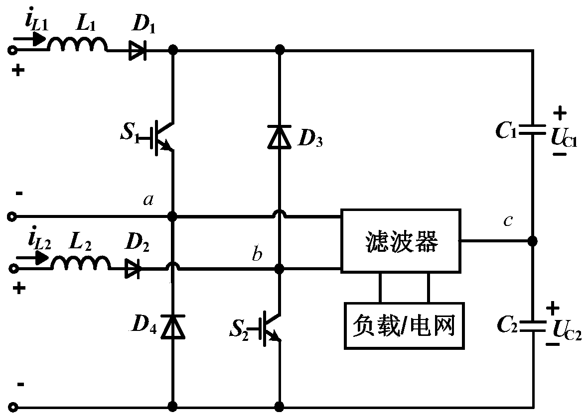
[0064] This embodiment relates to a control circuit of a dual-input boost inverter, which is applicable to a dual-input boost inverter in each technical solution described in Embodiment 1. The output side voltage of the filter is used as the feedback voltage, and the given voltage U ref The error value is obtained by comparison, and the error value is passed through the regulator (the type of regulator can be selected according to the needs, and the attached Figure 15 The example given in is the PID regulator, which can be selected in actual application, PI, PD, etc. are not limited by the examples listed in this embodiment and the accompanying drawings) After adjustment, it is compared with the triangular wave to generate a pulse signal, which is input to the power switch tube S 1 and S 2 the B side.

Embodiment 3

[0066] This embodiment proposes a control method for a dual-input boost inverter. The control method is a single-voltage closed-loop control, and the voltage on the output side of the filter is selected as the feedback voltage, which is equal to the given voltage U ref The error value is obtained by comparison, and the error value is adjusted by the regulator and compared with the triangular wave to generate a pulse signal to control the power switch tube S 1 and S 2 The turn-on and turn-off of the power switch tube S 1 and S 2 work in a complementary state.

[0067] To the power switch tube S 1 , S 2 The gate input control signal, the specific waveform is as Figure 6 As shown, from top to bottom is the power switch tube S 1 , S 2 gate input signal. The power switch tube S 1 and S 2 B terminal input bipolar modulation waveform, the working mode is as Figure 7-10 As shown, the timing diagram is as Figure 11 shown, with Figure 7-10 The same line type is a closed...


PUM


Abstract

The invention discloses a control method of a dual-input boost inverter, which belongs to the technical field of power electronic converters. Inductance L in the inverter of the present invention 1 Connect one end to the input power supply U in1 One end, the inductance L 1 The other end is connected to the diode D 1 anode connected; diode D 1 The cathodes are respectively connected to the power switch tube S 1 Terminal A, diode D 3 Cathode and Capacitor C 1 One end; capacitor C 1 The other end is connected to the capacitor C 2 One end of the inductance L 2 Connect one end to the input power supply U in2 One end, the inductance L 2 The other end is connected to the diode D 2 anode connected; diode D 2 The cathodes are respectively connected to the power switch tube S 2 A terminal and diode D 3 Anode: Aiming at the problems of many switching devices, complex structure and control, and single input power supply in the boost inverter of the prior art, the present invention adopts dual power supply, which can realize seamless switching of two power supplies and ensure boosting The normal operation of the inverter improves the stability of the system; in addition, fewer switching devices are required, the power density is high, and the cost can be saved.

Description

technical field [0001] The invention relates to the technical field of power electronic converters, in particular to a double-input boost inverter and its control circuit and method. Background technique [0002] With the rapid development of new energy power generation systems, the performance requirements of inverters are also getting higher and higher. Grid-connected inverter is the main interface device between grid and photovoltaic array, and its performance determines the performance of the entire photovoltaic power generation system. The pursuit of high reliability, high power density, high efficiency and high-quality waveform output is the development trend of inverters. [0003] The traditional bridge inverter has the characteristics of simple topology and low cost, so it is widely used, but the upper and lower switching tubes of the same bridge arm have a shoot-through situation, which reduces the reliability of the system; in order to prevent the occurrence of the...

Claims


Application Information

Patent Timeline
Patent Type & Authority Patents(China)
IPC IPC(8): H02M7/48
CPCH02M7/48H02M1/0083
Inventor 胡雪峰俞志祥戴冠军刘行张梦程宇
Owner ANHUI UNIVERSITY OF TECHNOLOGY
Why Eureka
Try Eureka