Double-input double-boost leakage-current-free inverter, and control circuit and method thereof

A dual-boost, leakage current technology, applied in the conversion of AC power input to DC power output, electrical components, photovoltaic power generation, etc., can solve the impact of system reliability and safety, increase the efficiency of the protection circuit system, and cannot meet a wide range of needs and other problems, to achieve the effect of increasing the volume and circuit design cost, cumbersome design, and small space occupation

Active Publication Date: 2021-11-02
NANJING UNIV OF INFORMATION SCI & TECH
View PDF6 Cites 0 Cited by
  • Summary
  • Abstract
  • Description
  • Claims
  • Application Information

AI Technical Summary

Problems solved by technology

However, these topologies have low boosting capacity, and the structure itself has leakage current problems, which affect the reliability and safety of the system. Generally, it is necessary to add protection circuits such as transformers or common-mode inductors to achieve electrical isolation and reduce leakage currents, or to control The method is designed to achieve a constant common-mode voltage to suppress the leakage current
Adding a protection circuit will affect the system efficiency and increase the cost of the inverter, and the design of the control strategy is generally more complicated and difficult to implement
[0005] Chinese invention patent application, publication number: CN107834886A; publication date: March 23, 2018; discloses a single-stage boost inverter and its control method, the application adds a boost inductor to the input DC power supply side, not only It realizes the voltage boost and solves the complex characteristics of the two-stage circuit. Its shortcoming is that the inverter has greatly changed the full-bridge inverter. The starting point is to realize the voltage boost function of the inverter. However, more switching devices are used, which increases the volume of the circuit, increases the loss, and reduces the efficiency of the inverter.
The structure of the above papers will generate leakage current when it works, the application scenarios are limited, and it cannot meet a wide range of needs

Method used


Image

  • Double-input double-boost leakage-current-free inverter, and control circuit and method thereof
  • Double-input double-boost leakage-current-free inverter, and control circuit and method thereof
  • Double-input double-boost leakage-current-free inverter, and control circuit and method thereof

Examples


Embodiment 1

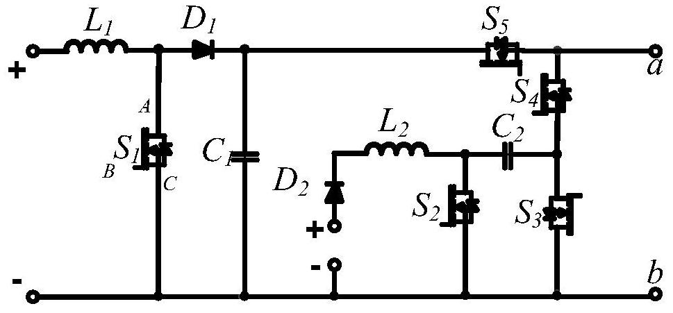
[0070] like figure 1 As shown, this embodiment proposes a dual-input dual-boost non-leakage current inverter, including a switch tube S 1 , switch tube S 2 , switch tube S 3 , switch tube S 4 , switch tube S 5 , Diode D 1 , Diode D 2 , inductance L 1 , inductance L 2 , inductance C 1 and inductance C 2 ; Among them, the input power U in1 Connect one end of the inductor L 1 One end, the inductance L 1 The other end is connected to the diode D 1 Anode and switch tube S 1 The A terminal is connected; the diode D 1 The cathode is connected to the switching tube S 5 A terminal and capacitor C 1 One end of the input power supply U in2 One end of the diode D is connected 2 anode of the diode D 2 The cathode and the inductance L 2Connected to one end; inductance L 2 The other end is connected to the switch tube S 2 A terminal and capacitor C 2 One end of the capacitor C 2 The other end of the switch tube S 3 The C terminal and the switch tube S 4 The C termin...

Embodiment 2

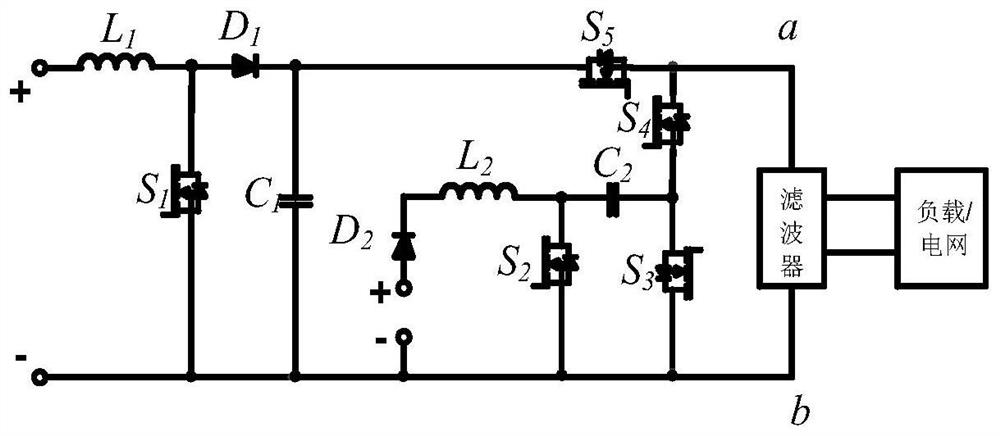
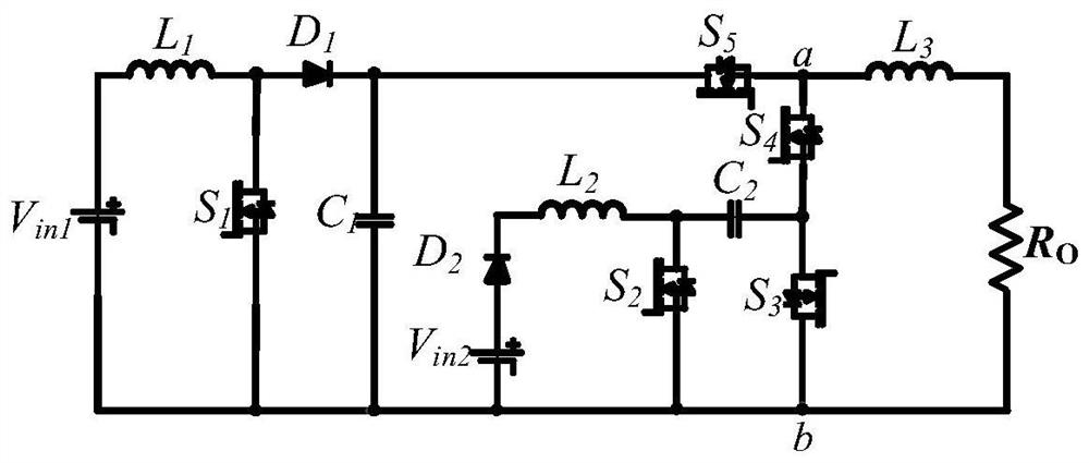
[0078] This embodiment relates to a control circuit of a double-input double-boost non-leakage current inverter. image 3 as shown, image 3 for figure 2 Schematic diagram of the circuit topology using filter I for medium filter selection, filter I includes filter inductor L 3 , filter inductance L 3 One end is connected to node a, and the filter inductor L 3 The other end is connected to node b; filter inductance L 3 The other end and node b form the output side of filter I.

Embodiment 3

[0080] This embodiment relates to a control circuit of a double-input double-boost non-leakage current inverter. The basic structure is the same as that of Embodiment 1, and the filter is filter II, as Figure 4 as shown, Figure 4 for figure 2 Schematic diagram of the circuit topology using filter II for medium filter selection, filter II includes filter inductor L 30 and filter capacitor C 0 , filter inductance L 30 One end is connected to node a, and the filter inductor L 30 the other end and the filter capacitor C 0 Connected at one end, the filter capacitor C 0 The other end is connected to node b, filter capacitor C 0 Terminal one and node b form the output side of filter II.


PUM


Abstract

The invention discloses a double-input double-boost leakage-current-free inverter, and a control circuit and method thereof, and belongs to the technical field of power electronic converters. One end of an inductor L1 of the inverter is connected with the positive electrode of an input power supply Uin1, and the other end of the inductor L1 is connected with the A end of a switching tube S1 and the positive electrode of a diode D1. The cathode of the diode D1 is connected with one end of a capacitor C1 and the A end of a switching tube S5; the other end of the capacitor C1, the negative electrode of the input power supply Uin1, the negative electrode of the input power supply Uin2, the C end of the switching tube S1, the C end of the switching tube S2 and the A end of the switching tube S3 are all connected with an output node b; the anode of the diode D2 is connected with the positive electrode of the input power supply Uin2 and one end of the inductor L2; the other end of the inductor L2 is connected with one end of the capacitor C2 and the A end of the switching tube S2; the other end of the capacitor C2 is connected with the C end of the switching tube S3 and the C end of the switching tube S4; and the A end of the switching tube S4 and the C end of the switching tube S5 are connected and jointly connected to an output node a. Double power supplies are adopted for power supply, control is simple, a step-up ratio is high, and the problem of current leakage is avoided.

Description

technical field [0001] The invention belongs to the technical field of power electronic converters, and more specifically relates to a double-input double-boost non-leakage current inverter and its control circuit and method. Background technique [0002] With the rapid development of new energy power generation systems, the performance requirements of inverters are also getting higher and higher. Grid-connected inverter is the main interface device between grid and photovoltaic array, and its performance determines the performance of the entire photovoltaic power generation system. The pursuit of high reliability, high power density, high efficiency and high-quality waveform output is the development trend of inverters. [0003] The traditional bridge inverter has the characteristics of simple topology and low cost, so it is widely used, but the traditional bridge inverter has no boost function, and a two-stage circuit is required in the new energy power generation system t...

Claims


Application Information

Patent Timeline
Patent Type & Authority Applications(China)
IPC IPC(8): H02M7/5387H02M1/44
CPCH02M7/53871H02M1/44Y02E10/56
Inventor 胡雪峰毛鹏丁新平王艳杰
Owner NANJING UNIV OF INFORMATION SCI & TECH
Why Eureka
Try Eureka