
Vertical cavity surface emitting laser and manufacturing method thereof

A vertical-cavity surface-emitting, manufacturing method technology, applied in the field of vertical-cavity surface-emitting lasers, can solve the problems of similar refractive index and low light extraction efficiency of VCSEL, and achieve the effect of improving light extraction efficiency and enhancing light reflection effect

Inactive Publication Date: 2019-08-16
HC SEMITEK SUZHOU
View PDF4 Cites 7 Cited by
  • Summary
  • Abstract
  • Description
  • Claims
  • Application Information

AI Technical Summary

Problems solved by technology

[0006] Embodiments of the present invention provide a vertical cavity surface emitting laser and a manufacturing method thereof, which can solve the problems in the prior art that the refractive index of the upper DBR and the lower DBR are similar, and the front light extraction efficiency of the VCSEL is low

Method used


Image

  • Vertical cavity surface emitting laser and manufacturing method thereof
  • Vertical cavity surface emitting laser and manufacturing method thereof
  • Vertical cavity surface emitting laser and manufacturing method thereof

Examples


Embodiment Construction

[0029] In order to make the object, technical solution and advantages of the present invention clearer, the implementation manner of the present invention will be further described in detail below in conjunction with the accompanying drawings.

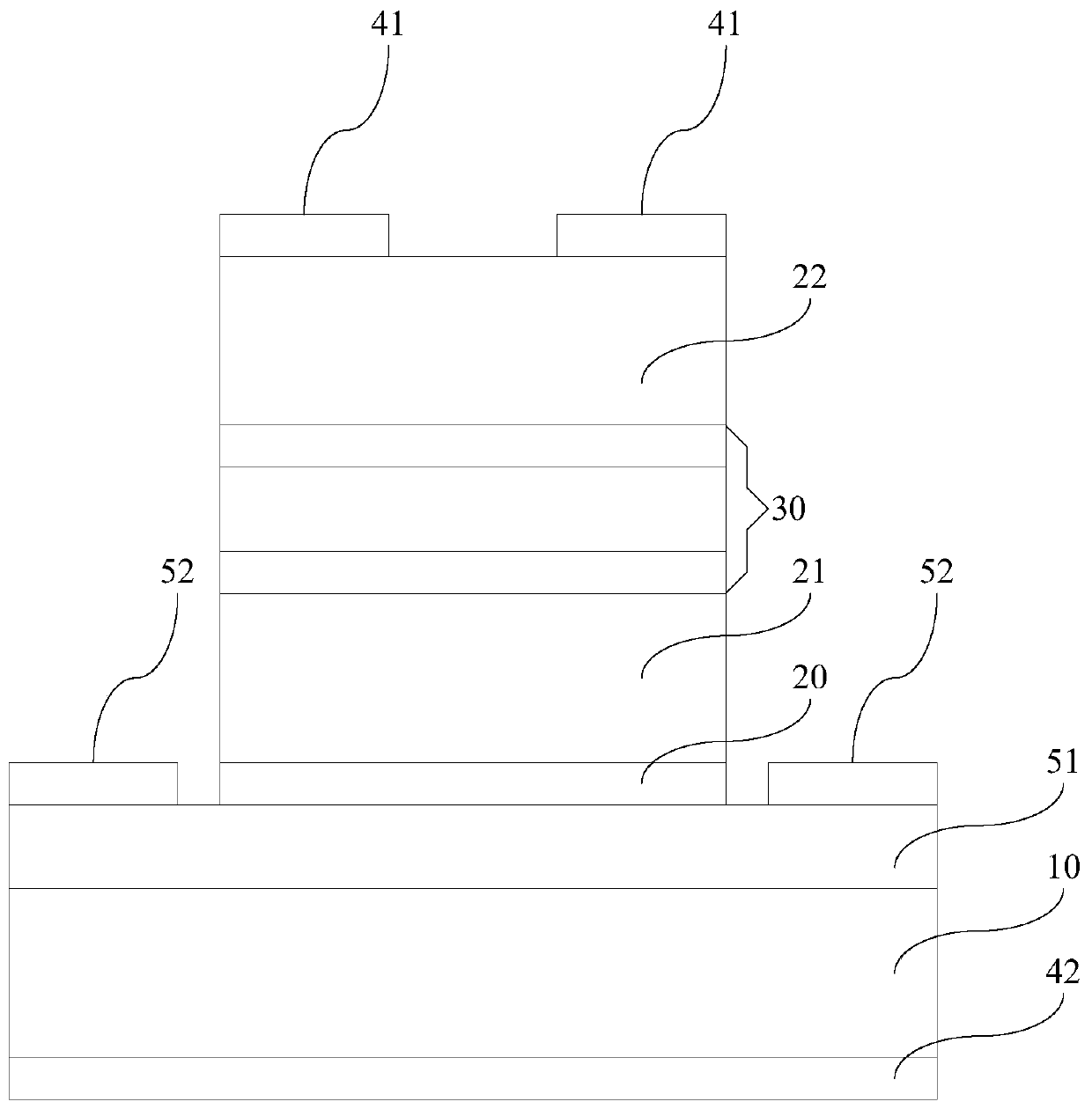
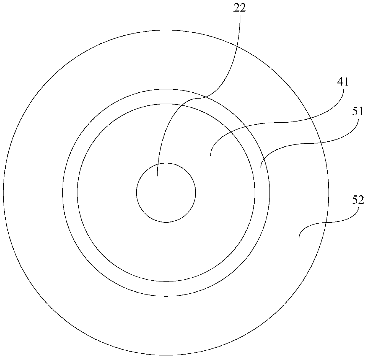
[0030] An embodiment of the present invention provides a vertical cavity surface emitting laser. figure 1 A schematic structural diagram of a vertical cavity surface emitting laser provided by an embodiment of the present invention. see figure 1 , the vertical cavity surface emitting laser comprises a substrate 10, a heat dissipation layer 20, a lower reflective layer 21, a light emitting region 30, an upper reflective layer 22, an upper metal electrode 41 and a lower metal electrode 42, the heat dissipation layer 20, the lower reflective layer 21, the light emitting The region 30, the upper reflective layer 22 and the upper metal electrode 41 are sequentially stacked on the first surface of the substrate 10, the lower metal electrode...


PUM

PropertyMeasurementUnit
thicknessaaaaaaaaaa
thicknessaaaaaaaaaa
thicknessaaaaaaaaaa

Abstract

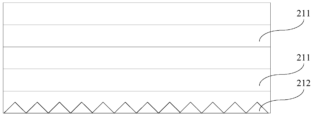
The invention discloses a vertical cavity surface emitting laser and a manufacturing method thereof, and belongs to the technical field of semiconductors. The vertical cavity surface emitting laser comprises a substrate, a heat dissipation layer, a lower reflection layer, a light emitting region, an upper reflection layer, an upper metal electrode and a lower metal electrode. The heat dissipationlayer, the lower reflection layer, the light emitting region, the upper reflection layer and the upper metal electrode are sequentially stacked on the first surface of the substrate, the lower metal electrode is arranged on the second surface of the substrate, and the second surface of the substrate is opposite to the first surface of the substrate; the lower reflecting layer comprises a pluralityof layers of boron alkene films which are sequentially stacked, and the heat dissipation layer is made of graphene or boron arsenide. According to the invention, the lower reflecting layer is changedinto a plurality of layers of boron alkene thin films which are sequentially stacked from a DBR (Distributed Bragg Reflection) structure, so that the reflecting effect of the bottom can be effectively enhanced, the reflectivity of the lower reflecting layer is far higher than that of the upper reflecting layer, and the light emitting efficiency of the VCSEL (Vertical Cavity Surface Emitting Laser) is greatly improved.

Description

technical field [0001] The invention relates to the technical field of semiconductors, in particular to a vertical cavity surface emitting laser and a manufacturing method thereof. Background technique [0002] Vertical Cavity Surface Emitting Laser (English: Vertical Cavity Surface Emitting Laser, VCSEL for short) is a semiconductor device based on gallium arsenide semiconductor material that emits laser light perpendicular to the top surface. Different from light emitting diodes (English: Light Emitting Diode, referred to as: LED), laser diodes (English: LaserDiode, referred to as: LD) and other light sources that need to be tested after the completion of production, VCSEL can be tested at any stage of production And to deal with the problems found in the test in time can effectively avoid the waste of production process and processing time. Moreover, VCSEL has the advantages of small size, circular output spot, single longitudinal mode output, low threshold current, low ...

Claims


Application Information

Patent Timeline
Patent Type & Authority Applications(China)
IPC IPC(8): H01S5/183H01S5/024
CPCH01S5/02461H01S5/18361H01S5/18375H01S2304/00
Inventor 葛永晖刘旺平曹阳王群吕蒙普胡加辉李鹏
Owner HC SEMITEK SUZHOU
Learn More