PCB components and manufacturing method thereof
A manufacturing method and technology of components, which are applied in the direction of electrical components, electrical components assembly printed circuits, printed circuit manufacturing, etc., can solve problems such as easy leakage of holes, inability to guarantee the heat dissipation effect of components, poor heat dissipation effect of components, etc.
- Summary
- Abstract
- Description
- Claims
- Application Information
AI Technical Summary
Problems solved by technology
Method used
Image

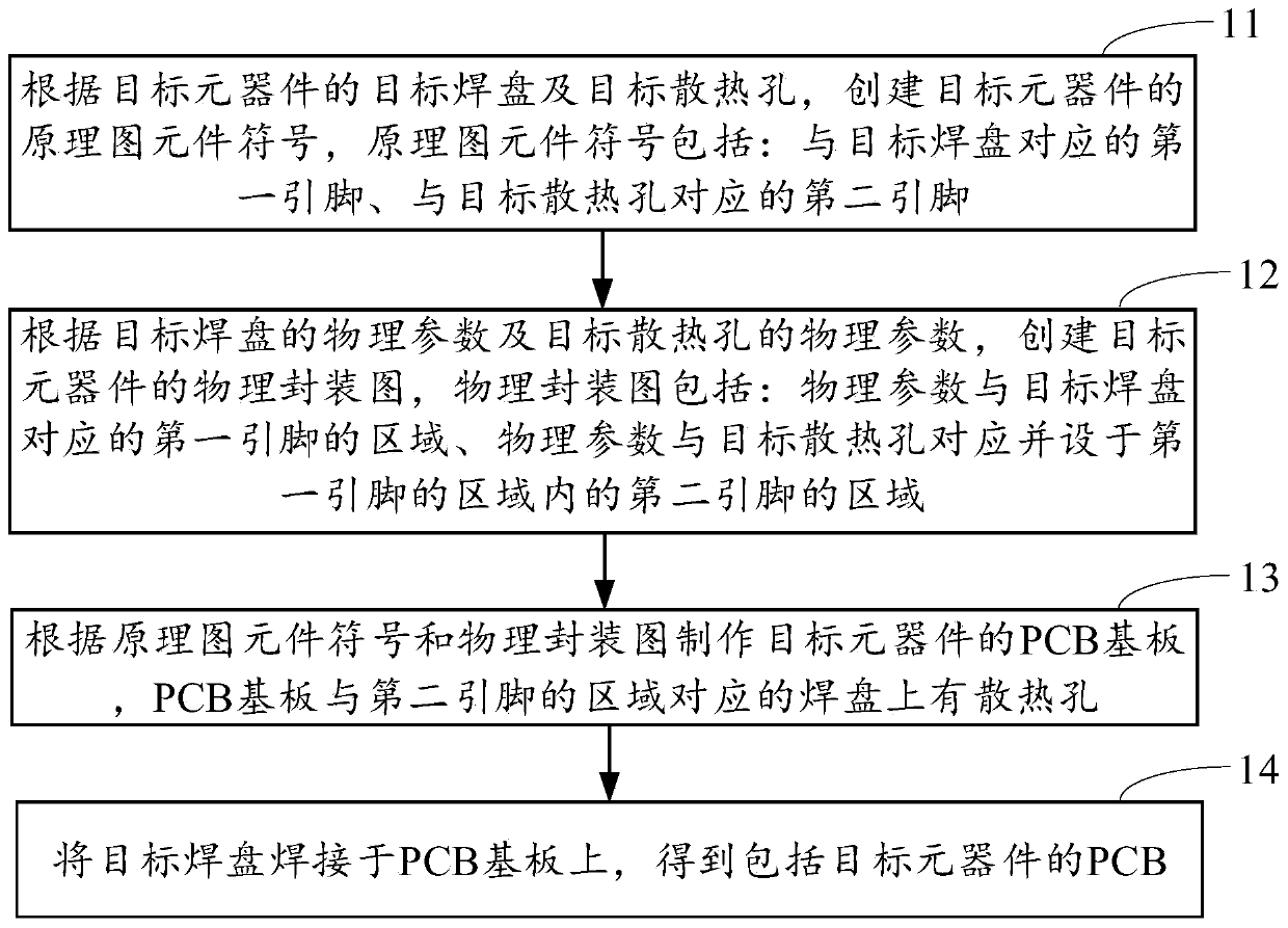
Examples
Embodiment Construction
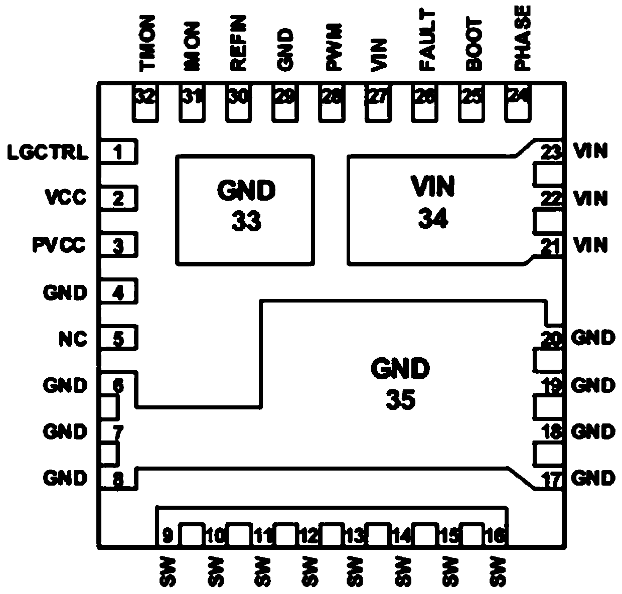
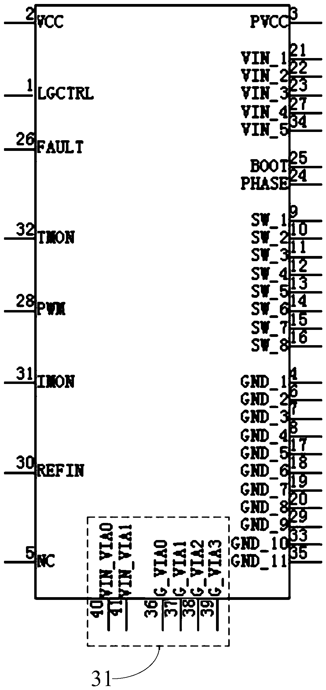
[0033] Reference will now be made in detail to the exemplary embodiments, examples of which are illustrated in the accompanying drawings. When the following description refers to the accompanying drawings, the same numerals in different drawings refer to the same or similar elements unless otherwise indicated. The implementations described in the following exemplary embodiments do not represent all implementations consistent with this application. Rather, they are merely examples of apparatuses and methods consistent with aspects of the present application as recited in the appended claims.
[0034] The terminology used in this application is for the purpose of describing particular embodiments only, and is not intended to limit the application. Unless otherwise defined, the technical terms or scientific terms used in the application shall have the ordinary meanings understood by those skilled in the art to which the application belongs. "First", "second" and similar words u...
PUM
 Abstract
Description
Claims
Application Information
 - R&D
- Intellectual Property
- Life Sciences
- Materials
- Tech Scout
- Unparalleled Data Quality
- Higher Quality Content
- 60% Fewer Hallucinations
Browse by: Latest US Patents, China's latest patents, Technical Efficacy Thesaurus, Application Domain, Technology Topic, Popular Technical Reports.
© 2025 PatSnap. All rights reserved.Legal|Privacy policy|Modern Slavery Act Transparency Statement|Sitemap|About US| Contact US: help@patsnap.com