Substrate for packaging high-power LED, manufacturing method of substrate, and packaging structure of substrate

A LED packaging and substrate manufacturing technology, which is applied in the direction of electrical components, circuits, semiconductor devices, etc., can solve the problems of poor longitudinal heat dissipation and application limitations of graphite layer heat dissipation, so as to improve the thermal conductivity, solve the problem of poor heat dissipation, and improve the service life Effect

Inactive Publication Date: 2019-08-09
UNIV OF ELECTRONICS SCI & TECH OF CHINA ZHONGSHAN INST
View PDF12 Cites 1 Cited by
  • Summary
  • Abstract
  • Description
  • Claims
  • Application Information

AI Technical Summary

Problems solved by technology

CN201721738604.1 discloses a substrate for high-power semiconductor packaging, including a graphite layer and a metal wiring layer for mounting chips. The metal wiring layer is fixed on one side of the graphite layer through an insulating adhesive, so that the graphite layer absorbs the chip. The generated heat achieves the effect of heat dissipation, but the graphite layer in this patent has better heat dissipation in the horizontal direction and poorer heat dissipation in the vertical direction. In the application field where high-power LED chips require high vertical heat dissipation capability, the heat dissipation application of the graphite layer is greatly restricted.

Method used


Image

  • Substrate for packaging high-power LED, manufacturing method of substrate, and packaging structure of substrate
  • Substrate for packaging high-power LED, manufacturing method of substrate, and packaging structure of substrate
  • Substrate for packaging high-power LED, manufacturing method of substrate, and packaging structure of substrate

Examples


Embodiment Construction

[0024] The following will clearly and completely describe the technical solutions in the embodiments of the present invention with reference to the accompanying drawings in the embodiments of the present invention. Obviously, the described embodiments are only some, not all, embodiments of the present invention. Based on the embodiments of the present invention, all other embodiments obtained by persons of ordinary skill in the art without making creative efforts belong to the protection scope of the present invention.

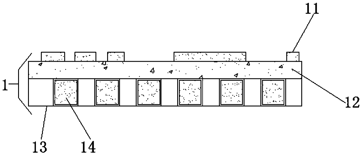
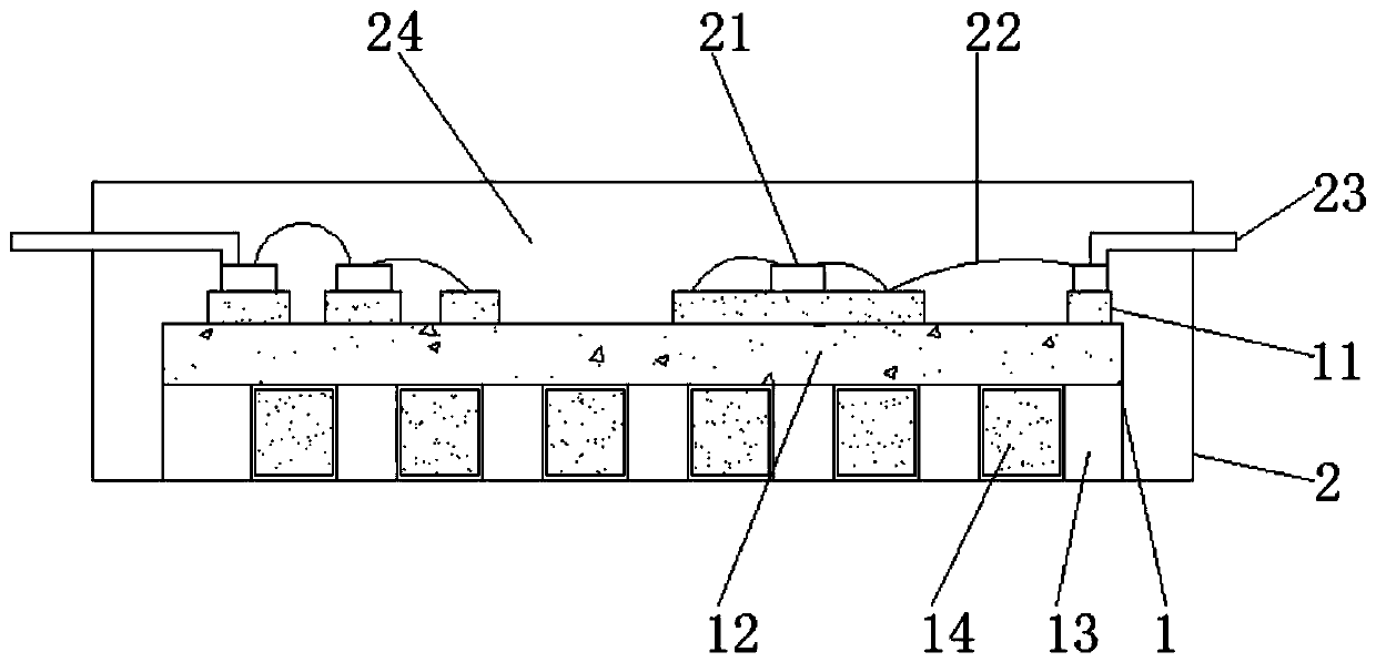
[0025] see figure 1 , the present invention provides a substrate for high-power LED packaging, comprising a substrate body (1), a copper circuit (11), a thermally conductive insulating layer (12), a graphite layer (13) and a graphene-coated metal block (14), The substrate body (1) includes a copper circuit (11), a thermally conductive insulating layer (12), a graphite layer (13) and a graphene-coated metal block (14), and graphene is not embedded in the graphi...


PUM

PropertyMeasurementUnit
Coating thicknessaaaaaaaaaa

Abstract

The invention relates to a substrate for packaging a high-power LED, a manufacturing method of the substrate and a packaging structure of the substrate. The substrate for packaging the high-power LEDcomprises a substrate and a packaging structure. A copper circuit, a heat-conducting insulating layer, a graphite layer and a metal block of a graphene coating are arranged on the substrate, and the packaging structure comprises an LED chip, a metal binding wire, a lead frame and packaging resin. The substrate is exposed out of one side of the packaging structure, and the LED chip and the circuitare connected through the metal binding wire, and the copper circuit and the lead frame are connected through the metal binding wire. The packaging resin is arranged at the outer side of the substrate. The invention discloses the substrate for packaging the high-power LED, the manufacturing method of the substrate and the packaging structure of the substrate. A metal insert with the graphene coating is arranged in the graphite layer, the longitudinal heat conduction coefficient of the graphite layer is greatly improved while the excellent transverse heat conduction characteristic of an original graphite layer is kept, the problem that the longitudinal heat dissipation capacity of the graphite layer is poor is solved, the temperature of an LED chip is reduced, and the service life of a packaging body is prolonged.

Description

technical field [0001] The invention relates to the technical field of high-power LED packaging, in particular to a substrate for high-power LED packaging, a manufacturing method for the substrate and a packaging structure thereof. Background technique [0002] With the development of the LED industry, high-power LEDs and their packaging structures have developed rapidly, and the packaging volume of high-power LEDs has become smaller and smaller. At the same time, the chip power inside the high-power LED package is increasing, resulting in packaging The body temperature rises higher and higher. As the temperature rises, if the LED's own chip cannot be dissipated quickly, it is easy to cause the wick chip to fail due to excessive temperature or the light decays seriously, thus greatly reducing the lifespan. The heating problem has been considered as one of the important technical problems faced by the packaging design of the high-power LED industry. Therefore, the heat diss...

Claims


Application Information

Patent Timeline
IPC IPC(8): H01L33/00H01L33/48H01L33/62H01L33/64
CPCH01L33/005H01L33/48H01L33/62H01L33/641
Inventor 王可徐梦雪王悦辉
Owner UNIV OF ELECTRONICS SCI & TECH OF CHINA ZHONGSHAN INST
Why Eureka
Try Eureka