Semiconductor structure and forming method thereof

A technology of semiconductor and conductive structure, applied in the field of semiconductor structure and its formation, can solve problems such as large contact resistance, achieve the effects of small parasitic capacitance, reduce resistance, and improve performance

Inactive Publication Date: 2019-07-09
SEMICON MFG INT (SHANGHAI) CORP +1
View PDF7 Cites 2 Cited by
  • Summary
  • Abstract
  • Description
  • Claims
  • Application Information

AI Technical Summary

Problems solved by technology

[0004] However, the semiconductor structure formed by the prior art still has the problem of high contact resistance between the metal silicide and the source-drain doped region

Method used


Image

  • Semiconductor structure and forming method thereof
  • Semiconductor structure and forming method thereof
  • Semiconductor structure and forming method thereof

Examples


Embodiment Construction

[0034] There are many problems in the semiconductor structure formed in the prior art, for example, the contact resistance between the conductive structure and the doped layer of the formed semiconductor structure is relatively large.

[0035] Now in combination with a semiconductor structure, the reason for the large contact resistance between the conductive structure and the doped layer of the semiconductor structure is analyzed:

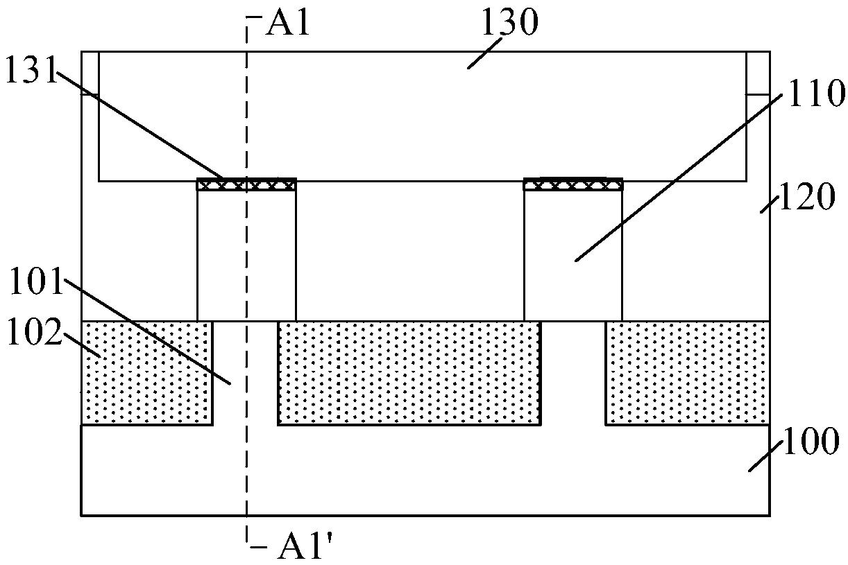
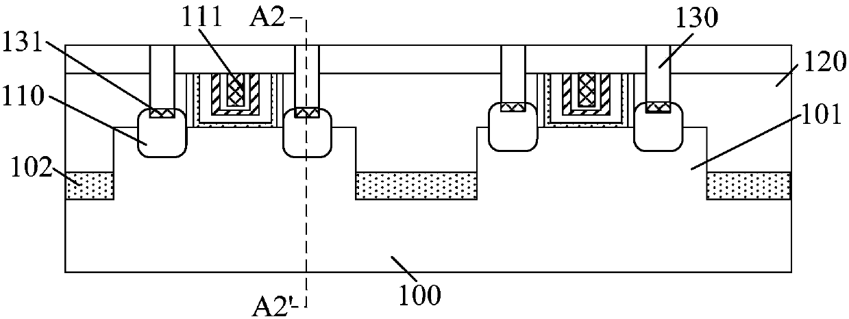
[0036] figure 1 and figure 2 is a structural schematic diagram of an embodiment of a semiconductor structure.

[0037] Please refer to figure 1 and figure 2 , figure 2 Yes figure 1 Sectional view along cutting line A1-A1', figure 1 Yes figure 2 A cross-sectional view along the cutting line A2-A2', the semiconductor structure includes: a substrate 100 with fins 101 thereon; an isolation structure 102 on the substrate 100, and the isolation structure 102 covers Part of the sidewall of the fin 101, and the surface of the isolation structu...


PUM

PropertyMeasurementUnit
thicknessaaaaaaaaaa
sizeaaaaaaaaaa
thicknessaaaaaaaaaa

Abstract

The invention discloses a semiconductor structure and a forming method thereof. The forming method includes the following steps of: forming a doped layer in a substrate or on the surface of the substrate, wherein the substrate exposes the side wall of the doped layer; forming a sacrificial layer on the surface of the side wall of the doped layer exposed by the substrate; forming a dielectric layeron the substrate and the doped layer, wherein the dielectric layer covers the side wall of the sacrificial layer; forming a first trench in the dielectric layer, wherein the bottom of the first trench exposes the top of the doped layer and the top of the sacrificial layer; after the first trench is formed, removing the sacrificial layer, and forming a second trench at the bottom of the first trench; forming a metallide on the surface of the doped layer exposed by the first trench and the second trench; and after the metallide is formed, forming plugs in the second trench and the first trench.According to the forming method, the resistance between the plugs and the doped layer can be reduced, and the performance of the semiconductor structure can be improved.

Description

technical field [0001] The invention relates to the technical field of semiconductor manufacturing, in particular to a semiconductor structure and a forming method thereof. Background technique [0002] With the continuous advancement of semiconductor technology, the feature size of semiconductor devices is gradually reduced. The reduction of critical dimensions means that more transistors can be arranged on the chip, and at the same time, higher requirements are placed on the semiconductor process. [0003] Because metal has good electrical conductivity, in semiconductor technology, the electrical connection between the source and drain doped regions and external circuits is usually realized through metal plugs. However, due to the large difference in the Fermi level between the metal and the semiconductor, the potential barrier between the metal plug and the source-drain doped region is relatively high, resulting in a relatively low contact resistance between the metal pl...

Claims


Application Information

Patent Timeline
Patent Type & Authority Applications(China)
IPC IPC(8): H01L21/76H01L21/762H01L29/06H01L29/10H01L29/36
CPCH01L21/76H01L21/762H01L29/0603H01L29/10H01L29/36
Inventor 周飞
Owner SEMICON MFG INT (SHANGHAI) CORP
Why Eureka
Try Eureka