
Chip input pin ESD protection circuit architecture with ultralow leakage current

An ESD protection, ultra-low leakage technology, applied in the electronic field, can solve the problems of reducing output impedance, ESD damage failure, increasing the secondary processing cost of sensors, etc., and achieve the effect of ultra-high input impedance performance and low-cost application

Active Publication Date: 2019-05-31
HANGZHOU SDIC MICROELECTRONICS
View PDF4 Cites 0 Cited by
  • Summary
  • Abstract
  • Description
  • Claims
  • Application Information

AI Technical Summary

Problems solved by technology

[0002] With the rapid development of the Internet of Things in recent years, the system-on-chip (SOC) needs to collect more and more types of sensors. Some sensors have relatively large internal resistance (such as PIR sensors), requiring the front-end signal acquisition input of the system-on-chip The terminal has an ultra-high input impedance (may need to reach the order of 1010), and the traditional chip input pin has an ESD protection device, and the large-sized ESD protection device has a certain leakage current, especially under high temperature conditions, the leakage current can reach 10 -9~10-8 order of magnitude, which cannot meet the ultra-high input impedance requirements of the sensor. If the ESD protection device on the input pin is removed, the chip is prone to ESD damage and failure. Therefore, the existing solutions generally require high internal resistance sensors and ultra-high The input impedance buffer device adopts special secondary processing and packaging, and finally reduces the output impedance to avoid the high impedance requirement of the front-end signal acquisition input end of the chip and ensure the ESD reliability of the chip
However, this solution not only increases the secondary processing cost of the sensor, but also brings additional device noise on the signal acquisition path, and is not conducive to the high integration of the system, which limits the high integration and low-cost development of IoT applications.

Method used


Image

  • Chip input pin ESD protection circuit architecture with ultralow leakage current
  • Chip input pin ESD protection circuit architecture with ultralow leakage current

Examples


Embodiment

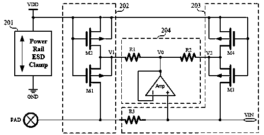
[0015] Such as figure 1 As shown, the patent of the present invention is an input pin ESD protection circuit architecture that can be integrated in a SOC chip to achieve ultra-high input impedance, which includes a power ground ESD clamp 201, a first-stage ESD protection module 202, a second stage ESD protection module 203 and leakage current transfer absorbing buffer 204 .

[0016] The power ground ESD clamper 201 realizes the real-time monitoring of the electrostatic pulse between the chip power supply and the ground, which can timely release the positive and negative electrostatic pulses between the power supply and the ground, and clamp the voltage between the power supply ground to the internal devices of the chip Within the acceptable safe voltage range, when there is no electrostatic pulse between the power supply and the ground, the power ground ESD clamp 201 does not affect the power supply of the chip power ground.

[0017] The first-level ESD protection module 202 ...


PUM


Abstract

The invention discloses a chip input pin ESD protection circuit architecture with ultralow leakage current. The chip input pin ESD protection circuit architecture with ultralow leakage current comprises a power ground ESD clamp, a first-stage ESD protection module, a second-stage ESD protection module and a leakage current transfer absorption buffer. The first-stage ESD protection module includesfirst and second PMOS transistors and a first voltage input terminal. The second-stage ESD protection module includes third and fourth PMOS transistors, a third resistor, a second voltage input terminal and a high-impedance input terminal. The leakage current transfer absorption buffer includes a first resistor, a second resistor, and an amplifier, and is configured to intercept the leakage current originally flowing to an input pin to implement zero input pin leakage current. The power ground ESD clamp has a positive terminal and a negative terminal, and has an electrostatic discharge capability for ESD positive and negative pulses between the power source and the ground. The chip input pin ESD protection circuit architecture can be integrated into a SOC chip to realize ESD protection ofthe input pin with ultrahigh input impedance.

Description

technical field [0001] The patent of the present invention relates to the field of electronics, in particular to an input pin ESD protection circuit architecture integrated in a SOC chip that can realize ultra-high input impedance. Background technique [0002] With the rapid development of the Internet of Things in recent years, the system-on-chip (SOC) needs to collect more and more types of sensors. Some sensors have relatively large internal resistance (such as PIR sensors), requiring the front-end signal acquisition input of the system-on-chip The terminal has an ultra-high input impedance (may need to reach the order of 1010), and the traditional chip input pin has an ESD protection device, and the large-sized ESD protection device has a certain leakage current, especially under high temperature conditions, the leakage current can reach 10 -9~10-8 order of magnitude, which cannot meet the ultra-high input impedance requirements of the sensor. If the ESD protection devi...

Claims


Application Information

Patent Timeline
IPC IPC(8): H01L27/02
Inventor 陈建章
Owner HANGZHOU SDIC MICROELECTRONICS
Learn More