Temperature-compensated crystal oscillator, and electronic device
A technology of quartz oscillator and temperature compensation circuit, which is applied to power oscillators, electrical components, etc., can solve the problem of increasing circuit scale, rising cost of temperature-compensating quartz oscillators, and difficulty in improving the oscillation characteristics of temperature-compensating quartz oscillators, etc. problem, to achieve the effect of expanding the variable range
- Summary
- Abstract
- Description
- Claims
- Application Information
AI Technical Summary
Problems solved by technology
Method used
Image
Examples
no. 1 approach
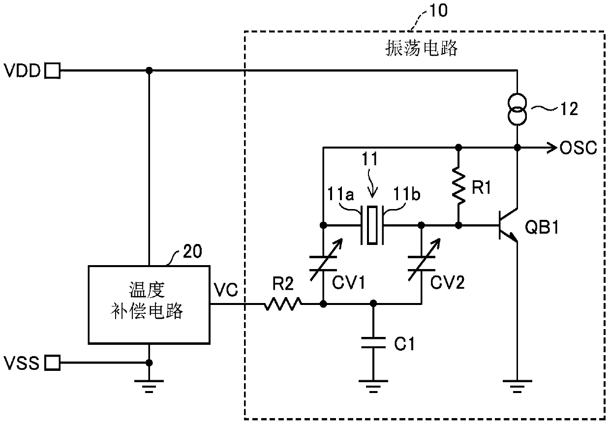
[0025] figure 1 It is a circuit diagram showing a configuration example of the temperature-compensated crystal oscillator according to the first embodiment of the present invention. This temperature-compensated crystal oscillator (TCXO) is supplied with a power supply potential VDD on the high potential side and a power supply potential VSS on the low potential side lower than the power supply potential VDD (in figure 1 In the illustrated example, the oscillating operation is performed at a ground potential of 0V), thereby generating an oscillating signal OSC.
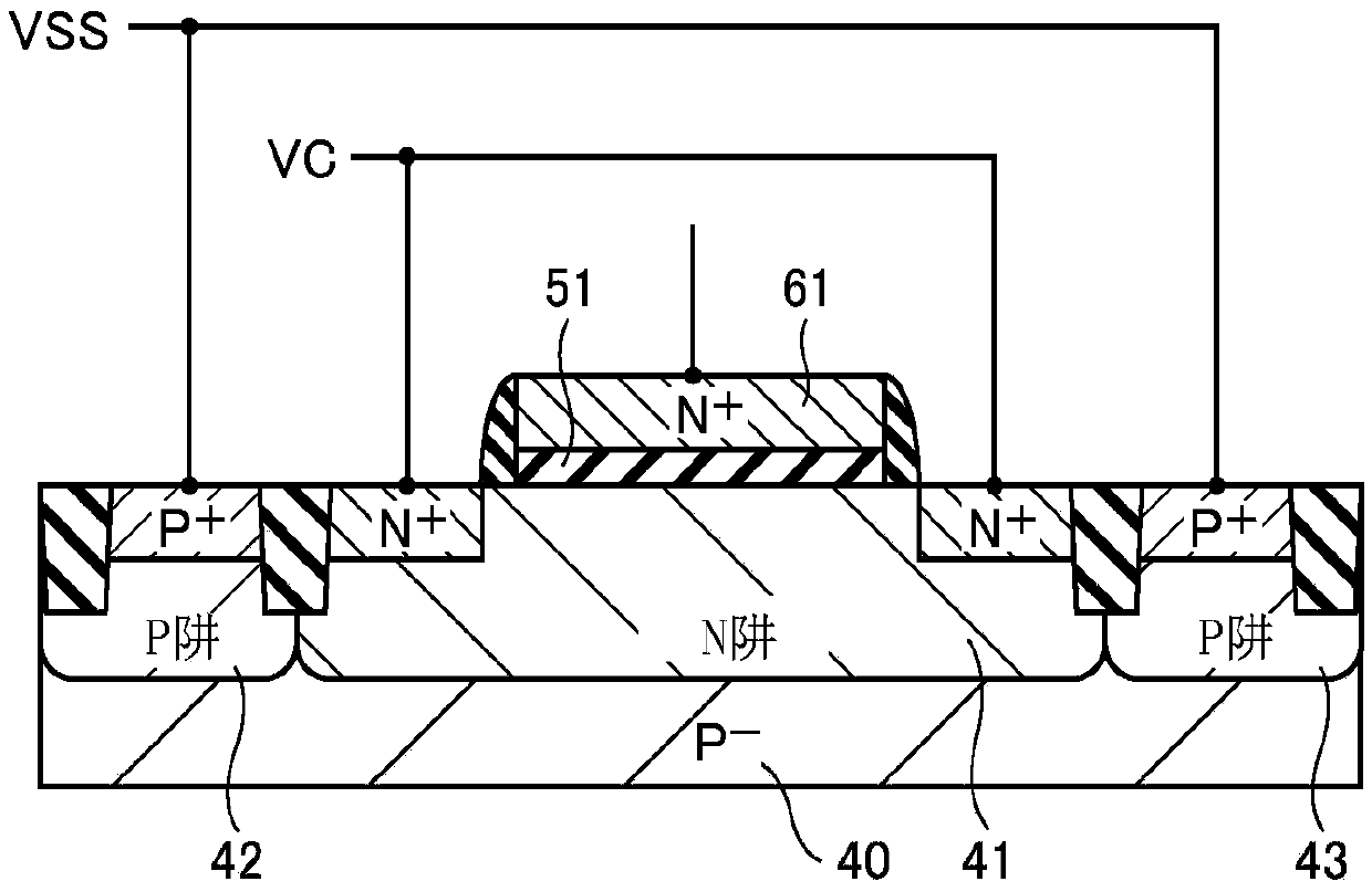
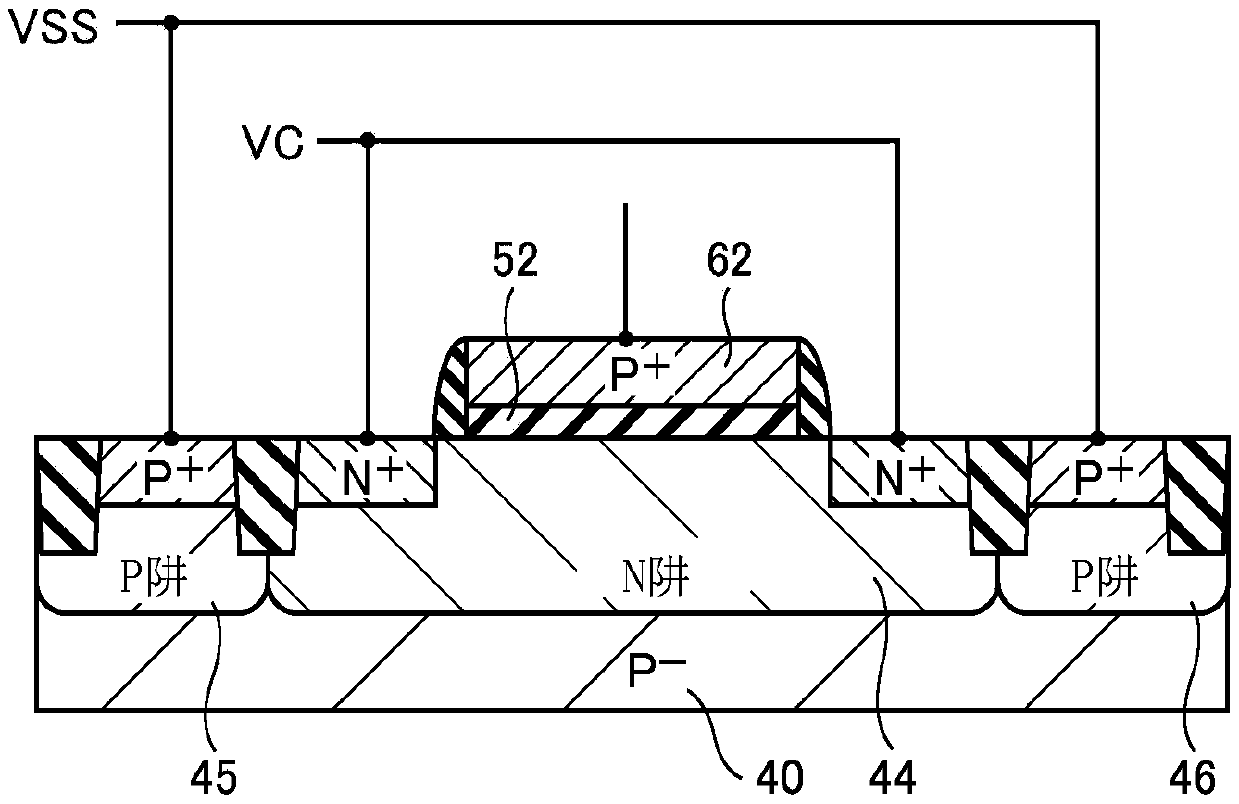
[0026] like figure 1 As shown, the temperature compensation type quartz oscillator includes an oscillation circuit 10 and a temperature compensation circuit 20 . The oscillation circuit 10 includes a crystal oscillator 11, a constant current source 12, an NPN bipolar transistor QB1, resistors R1 and R2, a first MOS type variable capacitance element CV1, a second MOS type variable capacitance element CV2, and a capaci...
no. 2 approach
[0048] In the second embodiment of the present invention, in figure 1 The structures of the first MOS type variable capacitance element CV1 and the second MOS type variable capacitance element CV2 used in the temperature-compensated crystal oscillator shown are different from those of the first embodiment. In other respects, the second embodiment may be the same as the first embodiment.
[0049] Image 6 It is a cross-sectional view showing a configuration example of the MOS-type variable capacitance element used in the second embodiment. like Image 6 As shown, an N well 47 and P wells 48 and 49 are arranged in the P-type semiconductor substrate 40 . In addition, an N-type contact region (N-type contact region (N + ), in the P wells 48 and 49, P-type contact regions (P + ).
[0050] For example, the first MOS type variable capacitance element CV1 has: a first back gate composed of an N well 47 arranged in the semiconductor substrate 40; and a first gate electrode 63 wit...
PUM
 Abstract
Description
Claims
Application Information
 - R&D Engineer
- R&D Manager
- IP Professional
- Industry Leading Data Capabilities
- Powerful AI technology
- Patent DNA Extraction
Browse by: Latest US Patents, China's latest patents, Technical Efficacy Thesaurus, Application Domain, Technology Topic, Popular Technical Reports.
© 2024 PatSnap. All rights reserved.Legal|Privacy policy|Modern Slavery Act Transparency Statement|Sitemap|About US| Contact US: help@patsnap.com


