
Nano-vacuum gap breakdown characteristic experimental device and method based on FIB-SEM two-beam system

A FIB-SEM and experimental device technology, applied in the field of experimental research systems, can solve the problem that optical microscopes cannot meet the resolution requirements and other problems

Inactive Publication Date: 2019-05-17
XI AN JIAOTONG UNIV
View PDF4 Cites 9 Cited by
  • Summary
  • Abstract
  • Description
  • Claims
  • Application Information

AI Technical Summary

Problems solved by technology

For micron and above scales, real-time observation and precise adjustment can be realized with the help of optical microscopes and mechanical displacement platforms; for nanoscales, optical microscopes can no longer meet the resolution requirements, and can only be carried out under electron microscopes

Method used


Image

  • Nano-vacuum gap breakdown characteristic experimental device and method based on FIB-SEM two-beam system
  • Nano-vacuum gap breakdown characteristic experimental device and method based on FIB-SEM two-beam system
  • Nano-vacuum gap breakdown characteristic experimental device and method based on FIB-SEM two-beam system

Examples


Embodiment Construction

[0030] The present invention is described in further detail below:

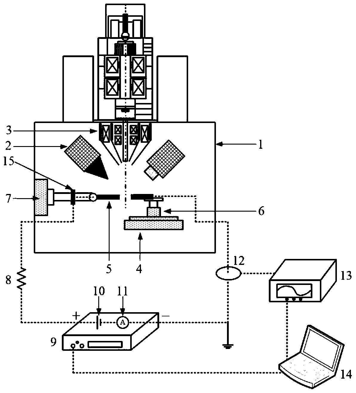
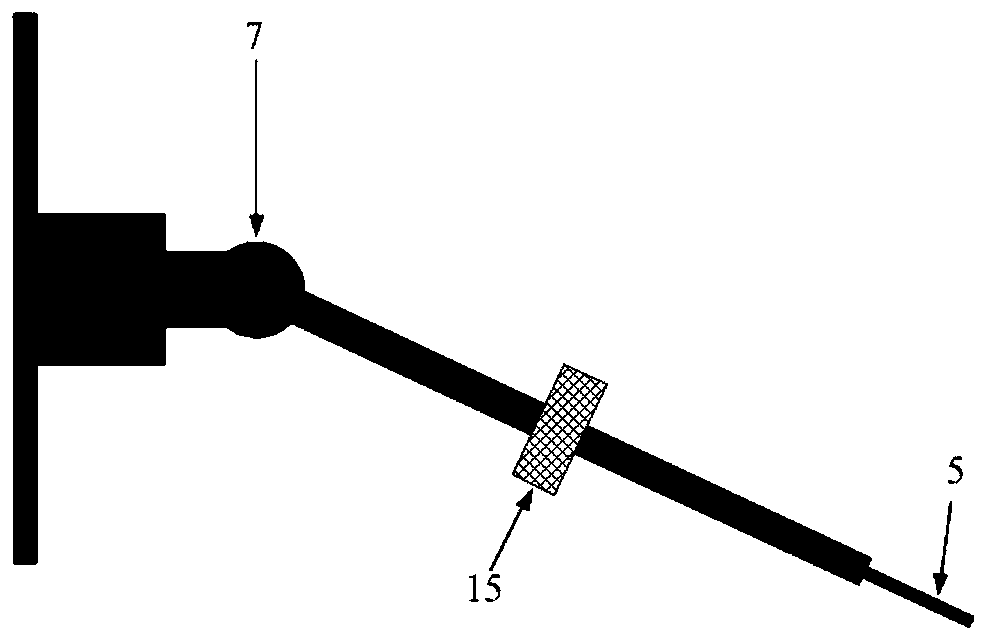
[0031] The nano-vacuum gap breakdown characteristics experimental device based on the FIB-SEM dual-beam system, including the FIB-SEM dual-beam system 1, the experimental chamber of the FIB-SEM dual-beam system 1 is equipped with a micro-nano scale electrode system 4, a micro-nano scale The nanomanipulator 7 and the five-axis sample stage 6 of the electrode system 4 are respectively connected to a test electrode 5, and the two test electrodes 5 are respectively connected to the voltage and current test circuit 9 through a current limiting resistor 8 and a pulse current sensor 12, and the pulse current sensor 12 Pass through the voltage and current test circuit 9 and connect with the oscilloscope 13, and the oscilloscope 13 and the voltage and current test circuit 9 are connected with the computer 14 to record the test data.

[0032]The FIB-SEM dual-beam system 1 is Helios Nanolab 600i model of FEI Company, th...


PUM


Abstract

The invention discloses a nano-vacuum gap breakdown characteristic experimental device and method based on an FIB-SEM two-beam system. The nano-vacuum gap breakdown characteristic experimental deviceincludes the FIB-SEM two-beam system. The FIB-SEM two-beam system is composed of a focused ion beam and a scanning electron microscope, a micro-nano scale electrode system is arranged in an experimental cavity of the FIB-SEM two-beam system, the micro-nano scale electrode system includes a test electrode, a nanometer manipulator and a five-axis sample table, the nanometer manipulator and the five-axis sample table are connected to a high-voltage voltage source and a weak current measurement unit in a voltage and current test circuit correspondingly through current limiting resistance, a pulsecurrent sensor passes through a test loop and is connected with an oscilloscope, and the oscilloscope and the voltage and current test circuit are connected with a computer to record test data. According to the nano-vacuum gap breakdown characteristic experimental device and method based on the FIB-SEM two-beam system, in-situ processing of a micro-nano-scale metal electrode, real-time regulationof vacuum gaps from 20 nm to 1 [mu]m, and corresponding functions of high-voltage testing and weak current measurement can be realized, and great significance for studying intrinsic rules of dischargebreakdown in the nano-scale vacuum gaps are achieved.

Description

technical field [0001] The invention relates to an experimental research system for studying the electrical characteristics and breakdown mechanism of nanoscale vacuum gaps, in particular to the electrical properties of nanoscale vacuum gap breakdown based on FIB (focused ion beam)-SEM (scanning electron microscope) dual-beam system Characteristic testing device and method. Background technique [0002] The study of electrical breakdown and insulation characteristics in nanoscale vacuum is a frontier topic in the field of high voltage and insulation technology. In recent years, with the further development of micro-nano processing technology, micro-nano-scale electrical components and electronic devices have emerged and been widely used in military and civilian fields. However, this type of micro-nano devices (such as NEMS, field emission display FED) often need to face a working environment with extremely high field strength, and its insulation reliability has received mor...

Claims


Application Information

Patent Timeline
Patent Type & Authority Applications(China)
IPC IPC(8): G01R31/12
Inventor 孟国栋成永红董承业应琪王科镜张笃佼
Owner XI AN JIAOTONG UNIV
Learn More