


Quick Research
Generate reliable direction feasibility study reports for your R&D in just a few steps.

Technical Q&A
Discover and master advanced knowledge NOW. Basics, ideas, possibilities, all at once.

Find Solutions
As an expert in R&D theories, this can generate solutions to your technical problems instantly.

Evaluate Feasibility
Analyze your overall solution with one click, know your potential R&D risks in advance.

Monitor Landscape
Get weekly tech updates, stay abreast of the latest tech innovations and key insights.
Array substrate, preparation method thereof, and display panel
An array substrate and substrate technology, which is applied to semiconductor/solid-state device parts, instruments, semiconductor devices, etc., can solve the problems of small aperture ratio and low yield rate, and achieve increased aperture ratio, improved yield rate, and good process compatibility Effect
- Summary
- Abstract
- Description
- Claims
- Application Information
AI Technical Summary
Problems solved by technology
Method used
Image

Examples
no. 1 example
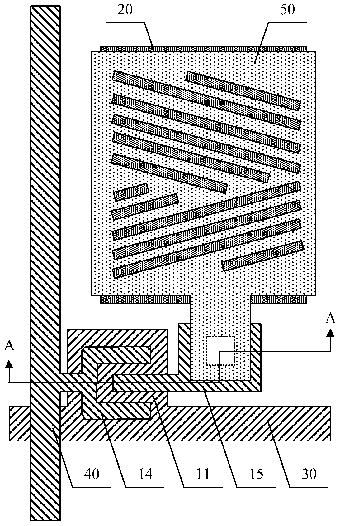
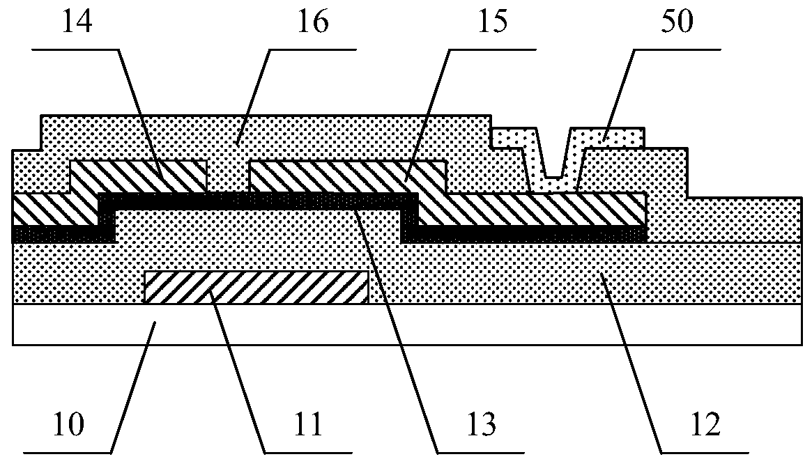
[0057] Figure 5 is a schematic structural diagram of the first embodiment of the array substrate of the present invention, Figure 6 for Figure 5 The cross-sectional view of A-A in the middle. Such as Figure 5 and Figure 6 As shown, the array substrate provided in this embodiment includes:
[0058] base 10;
[0059] A pixel electrode 50, a gate line 30 and a gate electrode 11 arranged on the substrate 10;
[0060] a gate insulating layer 12 covering the pixel electrode 50, the gate line 30 and the gate electrode 11;
[0061] The active layer 13, the source electrode 14, the drain electrode 15 and the data line 40 arranged on the gate insulating layer 12, a conductive channel is formed between the source electrode 14 and the drain electrode 15;
[0062] A passivation layer 16 covering the active layer 13, the source electrode 14, the drain electrode 15 and the data line 40, and a transfer via hole is opened on the passivation layer 16 to simultaneously expose the dra...
no. 2 example
[0073] Figure 13 It is a schematic diagram of the structure of the transfer via according to the embodiment of the present invention. Such as Figure 13 As shown, the transfer via hole is actually composed of half of the shallow hole (overlapping the drain electrode 15 ) and half of the deep hole (overlapping the pixel electrode 50 ), which is also called a half via (Half Via) design. Since the active layer and the source electrode / drain electrode are formed by a patterning process using a half-tone or gray-tone mask, there is a semiconductor film under the drain electrode 15, and the line width CD of the semiconductor film is greater than that of the drain electrode 15. The line width CD means that the active layer protrusion 131 exists. The active layer protrusions 131 appear because the wet etching method is used for the metal thin film, and the dry etching method is used for the semiconductor thin film, so the ends of the two cannot be guaranteed to be flush, resulting ...
no. 3 example
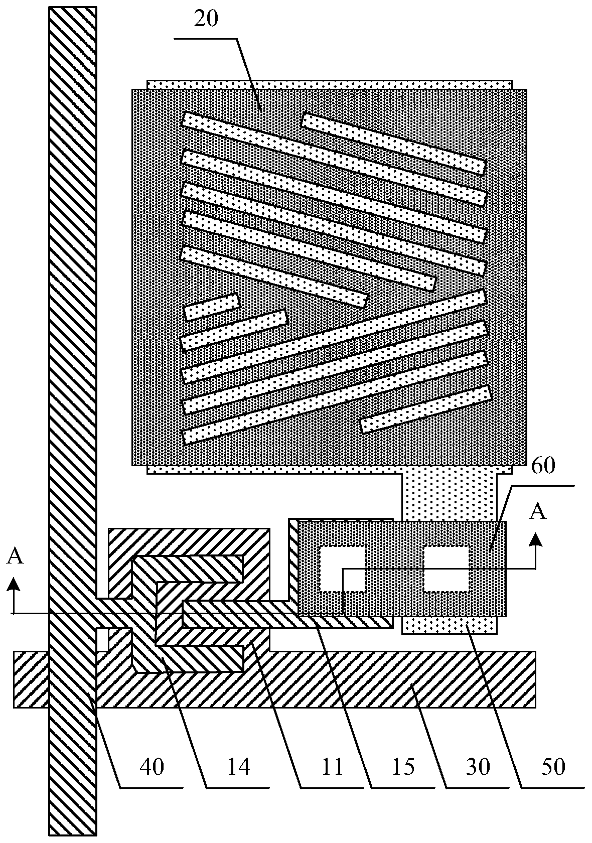
[0078] Figure 15 It is a schematic structural diagram of the third embodiment of the array substrate of the present invention. This embodiment is an extension of the aforementioned first embodiment. The main structure of the array substrate in this embodiment is the same as that of the aforementioned first embodiment. compensation block and a second compensation block. Such as Figure 15 As shown, in this embodiment, the first compensation block 60A is arranged on the side of the connection electrode 60 adjacent to the grid line 30, and the second compensation block 60B is arranged on the side of the connection electrode 60 away from the grid line 30, that is, both sides of the connection electrode 60 are Compensation blocks are provided. The structure of the first compensation block 60A is the same as that of the aforementioned second embodiment, and will not be repeated here. In the direction parallel to the data line 40, the orthographic projection of the second compen...
PUM
 Abstract
Description
Claims
Application Information
 - R&D Engineer
- R&D Manager
- IP Professional
- Industry Leading Data Capabilities
- Powerful AI technology
- Patent DNA Extraction
Browse by: Latest US Patents, China's latest patents, Technical Efficacy Thesaurus, Application Domain, Technology Topic, Popular Technical Reports.
© 2024 PatSnap. All rights reserved.Legal|Privacy policy|Modern Slavery Act Transparency Statement|Sitemap|About US| Contact US: help@patsnap.com