
Infrared transmitting high sensitivity visible light detector and preparation method thereof

A visible light and infrared transmission technology, applied in the field of photoelectric detection, can solve the problem of low sensitivity and achieve the effect of good transmission ability

Active Publication Date: 2019-05-10
XIAN TECHNOLOGICAL UNIV
View PDF7 Cites 3 Cited by
  • Summary
  • Abstract
  • Description
  • Claims
  • Application Information

AI Technical Summary

Problems solved by technology

Both visible and infrared detection are realized by the same photosensitive layer / heterojunction, resulting in lower sensitivity

Method used

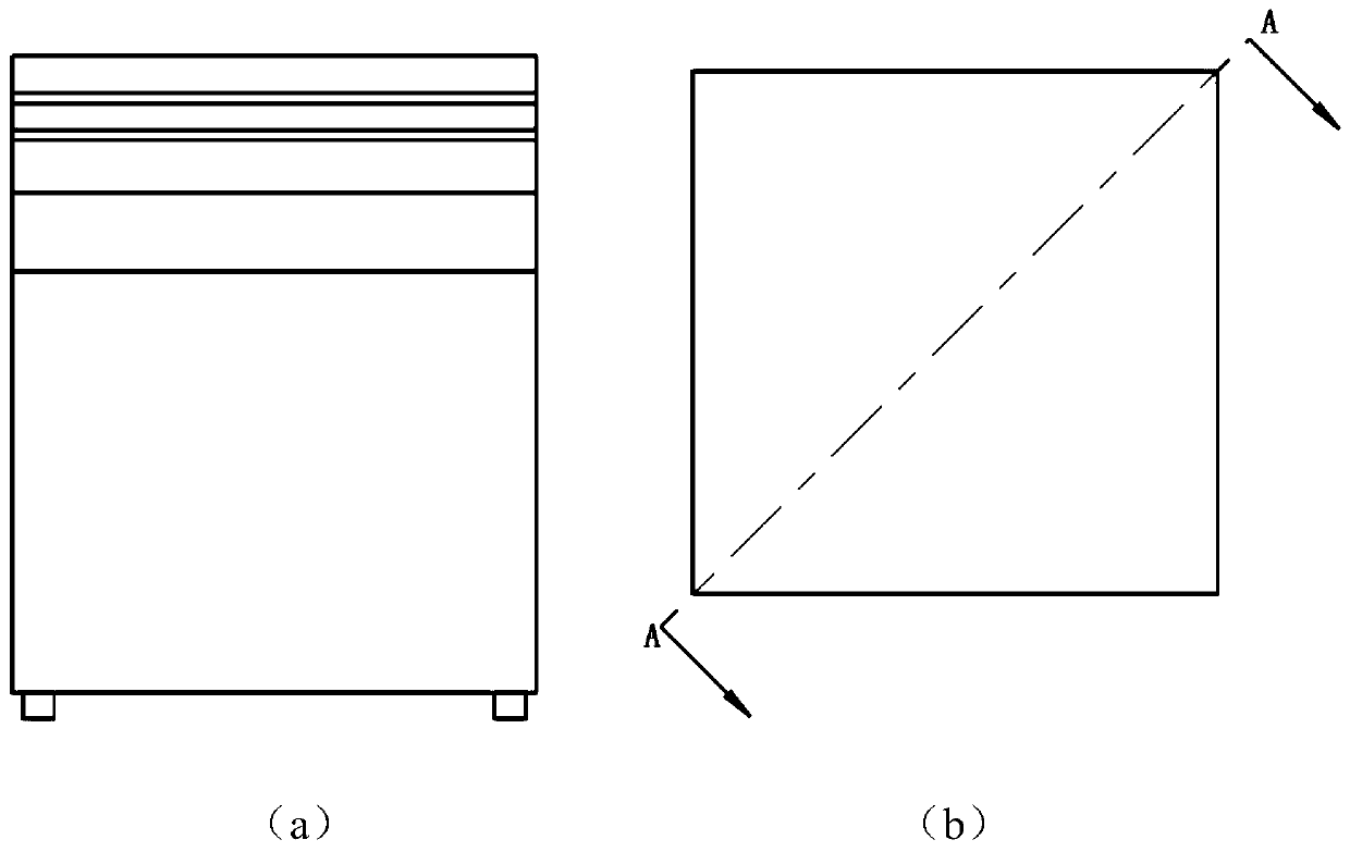

Image

  • Infrared transmitting high sensitivity visible light detector and preparation method thereof
  • Infrared transmitting high sensitivity visible light detector and preparation method thereof
  • Infrared transmitting high sensitivity visible light detector and preparation method thereof

Examples


Embodiment Construction

[0048] The present invention is described in further detail below in conjunction with accompanying drawing:

[0049] see figure 1 , the present invention discloses an infrared-transmitting high-sensitivity visible light detector and a preparation method thereof; the infrared-transmitting high-sensitivity visible light detector sequentially includes a passivation layer 14, an upper electrode 13, a heterojunction 15, The lower electrode 3 and the intrinsic single crystal silicon substrate 2; wherein, the heterojunction 15 includes a heterojunction upper layer 5 and a heterojunction lower layer 4;

[0050] The lower electrode 3 is silicon with conductive properties formed by heavily doping phosphorus, boron, and arsenic plasma below the upper surface of the intrinsic single crystal silicon wafer at a distance of 1-10 μm. The thickness of the lower electrode 3 is 2-20 μm. Both the lower heterojunction layer 4 and the intrinsic single crystal silicon substrate 2 are intrinsic sing...


PUM

PropertyMeasurementUnit
Thicknessaaaaaaaaaa
Thicknessaaaaaaaaaa
Thicknessaaaaaaaaaa

Abstract

The invention discloses an infrared transmitting high sensitivity visible light detector and a preparation method thereof. The detector is composed of a passivation layer, an upper electrode, a heterojunction, a lower electrode and an intrinsic monocrystalline silicon substrate. The upper electrode is made of a material which is conductive and is transparent to visible light and infrared. The heterojunction comprises an upper heterojunction layer and a lower heterojunction layer. The upper heterojunction layer is nano-film which is sensitive to the visible light and can transmit the infrared.The lower heterojunction layer is intrinsic monocrystalline silicon. When the visible light and the infrared transmit the upper electrode and the upper heterojunction layer, the visible light stimulates electron hole pairs in the heterojunction, the electron hole pairs are collected by the upper electrode and the lower electrode and are discharged from longitudinally set metal columns, and the infrared passes through a whole detection structure, so the visible light is detected, and moreover, transmission of the infrared is not influenced. Compared with a conventional structure, the detector has the advantages that distance between the electrodes and a junction area is low, so recombination rates of the electron hole pairs can be reduced before the electron hole pairs reach the electrodes,and collection efficiency of photon-generated carriers is improved. Through longitudinal metal structure design, light shielding is reduced, and sensitivity is improved.

Description

【Technical field】 [0001] The invention belongs to the technical field of photoelectric detection, and in particular relates to an infrared-transmitting high-sensitivity visible light detector and a preparation method thereof. 【Background technique】 [0002] With the development of industrial technology and living standards, people have put forward higher requirements for the amount of information contained in images. A single infrared imaging or a single visible light imaging can no longer meet the demand. Imaging technologies with wider bands are increasingly popular. Focus, especially on technologies that can simultaneously image visible and infrared light. [0003] Patent CN102866490B proposes a three-band optical imaging system of visible light, mid-wave infrared and long-wave infrared. The optical imaging system realizes three-band detection of visible light, mid-wave infrared and long-wave infrared. However, because the system uses a multi-channel, multi-chip imaging...

Claims


Application Information

Patent Timeline
IPC IPC(8): H01L31/109H01L31/0224H01L31/0336H01L31/18
CPCH01L31/109H01L31/036H01L31/028H01L31/02005H01L31/032H01L31/022408H01L31/1016H01L31/1868
Inventor 刘欢安妍刘卫国韩军蔡长龙白民宇王卓曼
Owner XIAN TECHNOLOGICAL UNIV
Learn More