Display substrate, manufacturing method thereof, and display device
A production method and technology for display substrates, which are applied in the manufacture of semiconductor/solid-state devices, electrical components, and electrical solid-state devices, etc., can solve the problems of cracks in the packaging film, reducing the reliability of the packaging film, and failure of the packaging film, so as to avoid failure and improve the Reliability and effect of ensuring film thickness uniformity
- Summary
- Abstract
- Description
- Claims
- Application Information
AI Technical Summary
Problems solved by technology
Method used
Image


Examples
no. 1 example
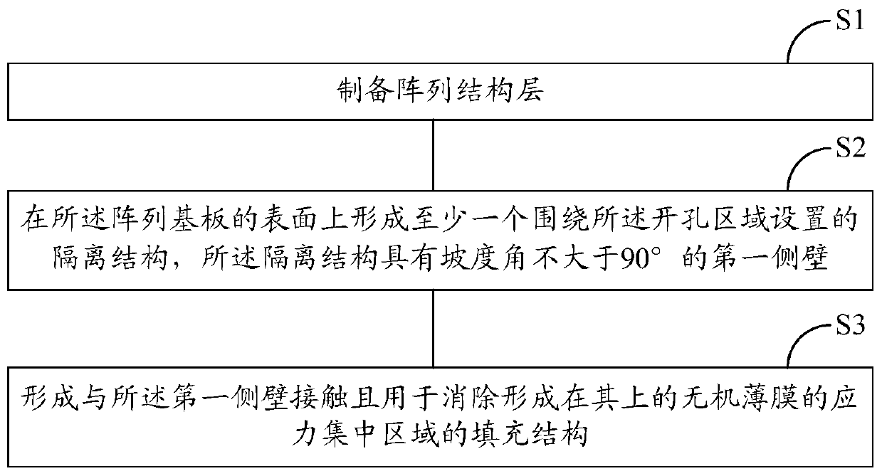
[0067] According to the first embodiment of the present invention, there is a method for manufacturing a display substrate. The display substrate includes a display area, and an opening area is arranged in the display area. The manufacturing method includes:
[0068] S1: preparing the array structure layer;
[0069] S2: forming at least one isolation structure disposed around the opening area on the surface of the array structure layer, the isolation structure having a first side wall with a slope angle not greater than 90°;
[0070] S3: forming a stress concentration region in contact with the first sidewall and used for eliminating the inorganic thin film formed thereon.
[0071] In this embodiment, before S3, it also includes forming a pixel defining layer and a light emitting structure layer; after S3, it also includes forming a first inorganic thin film covering the filling structure and the isolation structure.
[0072] The method for fabricating a display substrate acc...
no. 2 example
[0095] The second embodiment of the present invention is a method for manufacturing a display substrate. The display substrate includes a display area, and an opening area is arranged in the display area. The manufacturing method includes:
[0096] S1: preparing the array structure layer;
[0097] S2: forming at least one isolation structure disposed around the opening area on the surface of the array structure layer, the isolation structure having a first side wall with a slope angle not greater than 90°;
[0098] S3: forming a stress concentration region in contact with the first sidewall and used for eliminating the inorganic thin film formed thereon.
[0099] In this embodiment, before S3, it also includes forming a pixel defining layer, a light-emitting structure layer, and forming a first inorganic thin film covering the isolation structure; A protective layer; after S3, further comprising forming a second inorganic thin film covering the filling structure and the isola...
no. 3 example
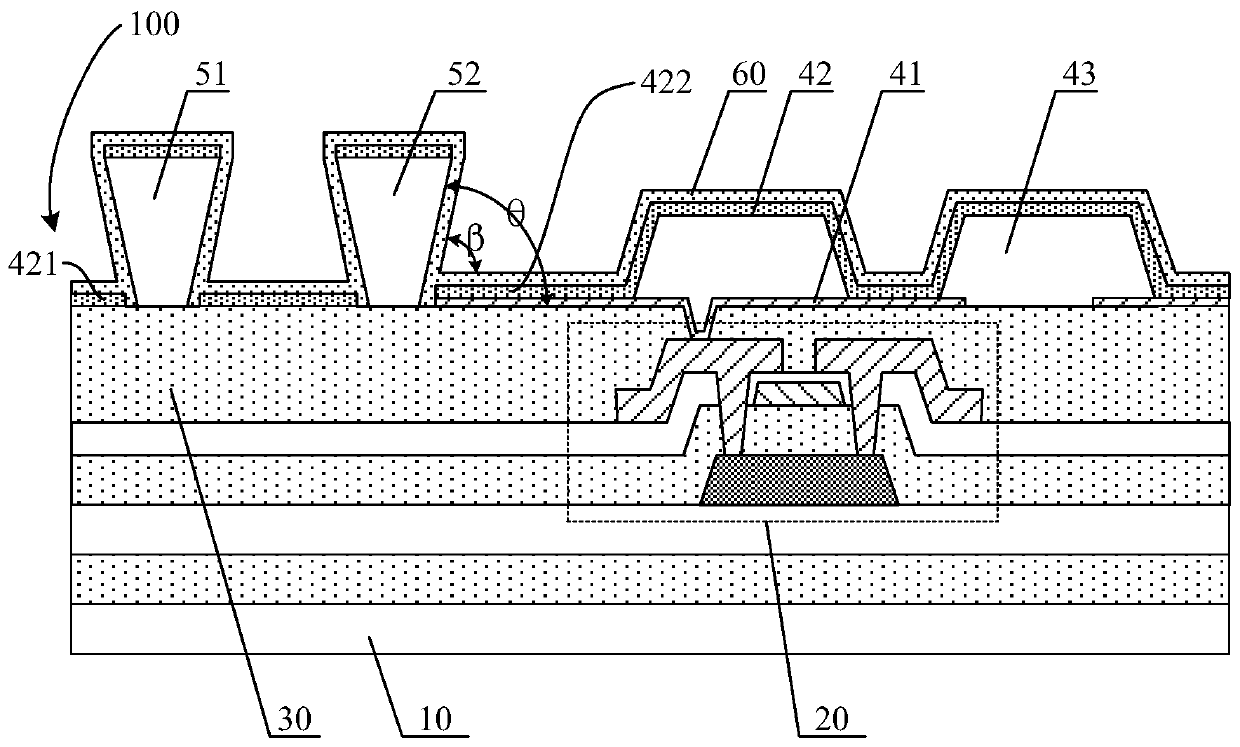
[0116] The third embodiment of the present invention provides a display substrate, such as figure 1 and Figure 12 As shown, the display substrate includes a display area, the display area is provided with an opening area 100, and an effective display area 200 outside the opening area 100, and the display substrate includes:
[0117] array structure layer;
[0118] an isolation structure disposed on the surface of the array structure layer and disposed around the opening area, the isolation structure has a first side wall with a slope angle not greater than 90°;
[0119] The filling structure 70 is in contact with the first sidewall and is used to eliminate the stress concentration area of the inorganic thin film formed thereon.
[0120] Wherein, the slope angle of the side wall of the filling structure 70 for carrying the inorganic thin film is not less than 90°.
[0121] Wherein, the array structure layer includes a substrate 10 , a thin film transistor 20 disposed on the...
PUM
 Abstract
Description
Claims
Application Information
 - R&D
- Intellectual Property
- Life Sciences
- Materials
- Tech Scout
- Unparalleled Data Quality
- Higher Quality Content
- 60% Fewer Hallucinations
Browse by: Latest US Patents, China's latest patents, Technical Efficacy Thesaurus, Application Domain, Technology Topic, Popular Technical Reports.
© 2025 PatSnap. All rights reserved.Legal|Privacy policy|Modern Slavery Act Transparency Statement|Sitemap|About US| Contact US: help@patsnap.com